


PCBA X-Ray Inspection Technology and Solder Defect Analysis
- Pubdate 2025-10-10
PCBA X-Ray Inspection Technology and Solder Defect Analysis
In modern electronics manufacturing, BGA and CSP packaging technologies are becoming increasingly popular, with devices becoming smaller and denser, and pins hidden beneath the component. Traditional optical inspection cannot check the quality of solder joints underneath the Printed Circuit Board Assembly (PCBA), hence X-ray inspection technology has emerged to meet this need.
Fundamental Principles of X-Ray Inspection
X-rays possess extremely strong penetrating power. Different material densities and thicknesses absorb X-rays to varying degrees. By analyzing the intensity changes of X-rays after passing through a sample, grayscale contrast images are formed to identify internal structures.
Based on material density characteristics, PCBA components can be divided into four categories:
Tin-lead alloy solder joints (high density, appear dark in images)
Metal packaging shells, ceramic packaging, chips (medium density)
Plastic packaging materials, silicon materials (low density, appear light in images)
Void, crack defects and PCB vias (X-rays pass through completely, appear brightest)
Inspection Process and Methods
Professional X-ray inspection employs a layered, progressive inspection strategy:
Global Scan: Overall inspection of PCBA and component layout
Local Magnification: Focus on suspicious areas
Tilt Imaging: Confirm defect nature through multi-angle observation
BGA Specific Inspection: Specifically for hidden solder joints using tilted inspection
Related Technology: Chip Solder Void X-Ray Inspection Method
Standardized Inspection Flowchart
To ensure inspection efficiency and accuracy, we have established a systematic inspection process for step-by-step identification of various soldering defects:

Inspection Area Division and Defect Types
X-ray inspection divides the PCBA into two main inspection areas: the component-covered area and the exposed area. Defects such as solder dross, solder balls, and PCB opens can appear in any area and require tilt imaging to exclude external interference.
Common surface defects include solder dross, solder balls, opens, and excessively large solder balls:

Critical Functional Defect Detection
Critical defects such as shorts and missing solder balls directly affect product function and are zero-tolerance defects. The image below shows typical issues such as short circuits, misalignment, missing solder balls, and insufficient solder:

Void Defect Quantitative Analysis
Void defects require precise measurement and evaluation. Modern X-ray inspection equipment integrates automatic void area calculation functions to quickly determine if voids exceed standard limits:

BGA Hidden Solder Joint Inspection Technology
The solder joints of BGA components are hidden underneath the component. During vertical imaging, BGA cold solder joint defects can easily be obscured by the shadow of the solder balls. Tilt imaging technology can effectively identify abnormal solder joints:

Normal solder joints appear cylindrical, while abnormal solder joints appear circular; they can be clearly distinguished through angled imaging:

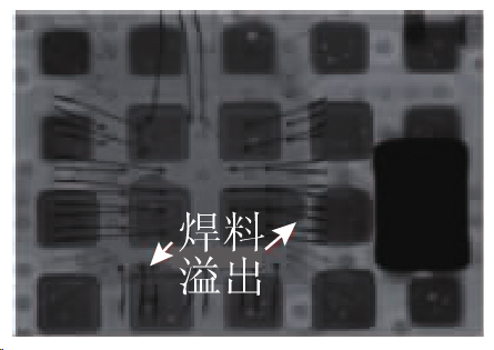
LGA Packaging Solder Quality Control
If the square contacts of LGA packaging are not pre-tinned, solder overflow can easily occur during reflow soldering. It is recommended to perform pre-tinning on the contacts to improve solder joint quality:
Technical Advantages Summary
Addressing the challenge of detecting hidden solder defects in PCBA, X-ray inspection technology provides a complete solution. Experimental verification shows that this technology can accurately identify various soldering defects, providing a basis for PCB design and process improvement.
Main Advantages: Clear imaging facilitating analysis, comprehensive defect coverage, efficient and standardized inspection process.