


Cross-Border Quality Trust: Turkish Firm Selects Wahfei Industrial X-Ray
This partnership with the Turkish client is just one milestone in Huafei’s global expansion. Backed by internationally aligned R&D, stringent manufacturing, and comprehensive cross-border after‑sales support, Huafei industrial X‑ray inspection systems have been exported to the U.S., France, Malaysia, Vietnam, and beyond. In advanced electronics workshops worldwide, our equipment reliably and efficiently safeguards our customers’ quality reputation.
View More
2026-07-09
How industrial X-Ray inspection equipment reveals hidden defects
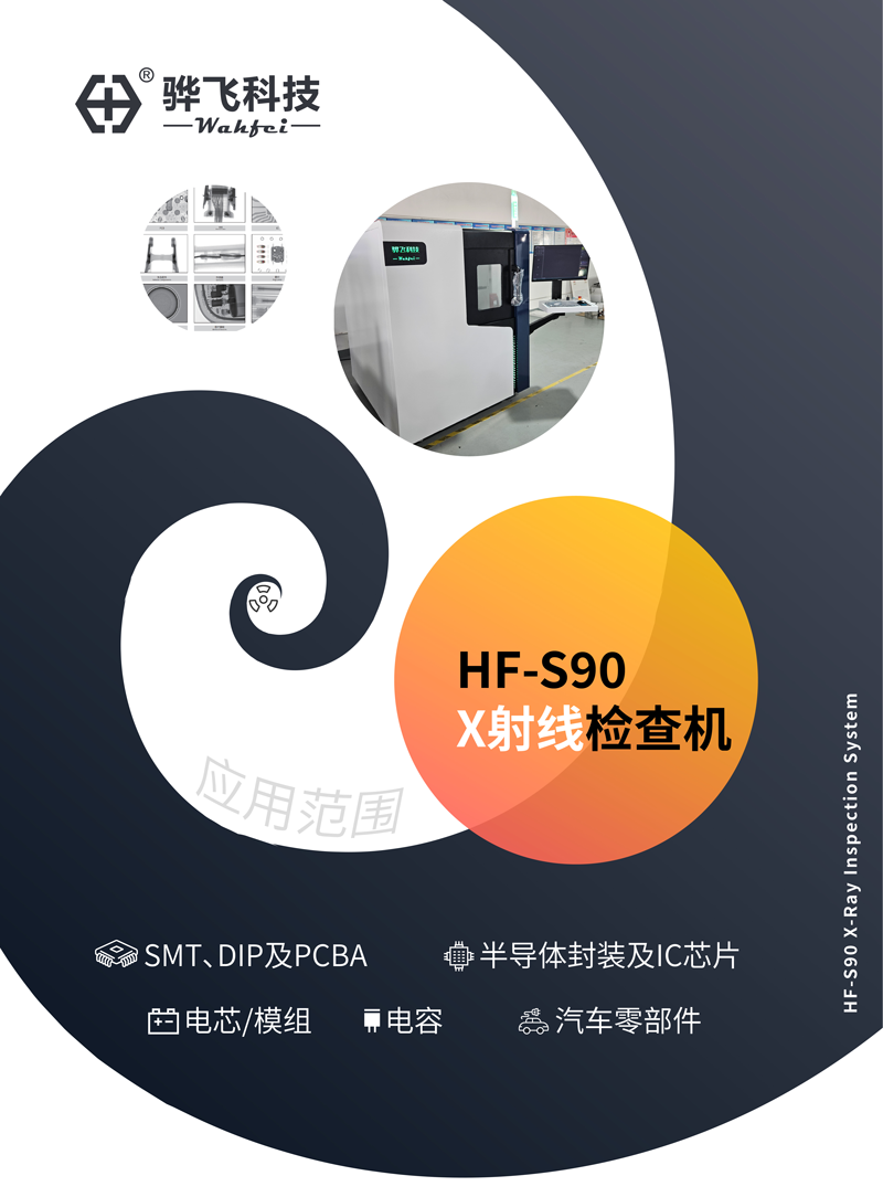
Products are getting smaller and their structures are becoming more and more complex - defects such as solder joints, bubbles, foreign objects, misalignment, and internal cracks, hidden inside the products, are invisible to the naked eye. By the time customers complain and bulk returns occur, irreversible losses have often been incurred. The Huafei HF-S90 is an industrial X-Ray inspection device specifically designed to address this pain point. Through non-destructive fluoroscopy imaging, it intuitively displays every detail inside the product on the screen, allowing the quality control team to make rapid and accurate quality judgments without dismantling or damaging the product.
View More
2026-07-04

Wahfei Technology Opens Suzhou Branch to Serve East China Clients Locally
To better serve East China manufacturers with instant local technical support, intelligent industrial X-ray equipment maker Huafei Technology launches its Suzhou Branch. With resident service staff and a full demo testing center, we offer ultra-fast local response and comprehensive NDT solutions.
View More
2026-06-29
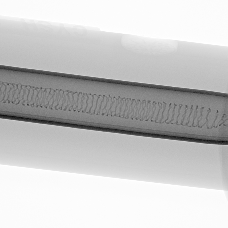
Actual X-Ray NDT images showing internal defects in heating wire
The penetrating power of X-rays makes them highly sensitive to density differences between metals and non-metals. In heating wire inspection, X-ray inspection systems can produce clear images and reliably detect the following types of defects:Core eccentricity / wire center offset-Broken wire / break points-Porosity / voids-Uneven winding pitch-Foreign material contamination-Joint defects-Cold solder joints or voids inside welded/crimped terminations-Unstable contact resistance …
View More
2026-06-16

Fuchang Precision (Belton-Technology) adopts industrial X-ray NDT to provide visual evidence for quality control of injection-molded products.
Fuchang Precision Products (Shenzhen) Co., Ltd. procures industrial X-ray inspection equipment for non-destructive testing of internal defects in injection-molded parts. Huafei Technology provides high-precision X-ray imaging solutions to enable intelligent upgrade of quality control for injection-molded products.
View More
2026-06-06
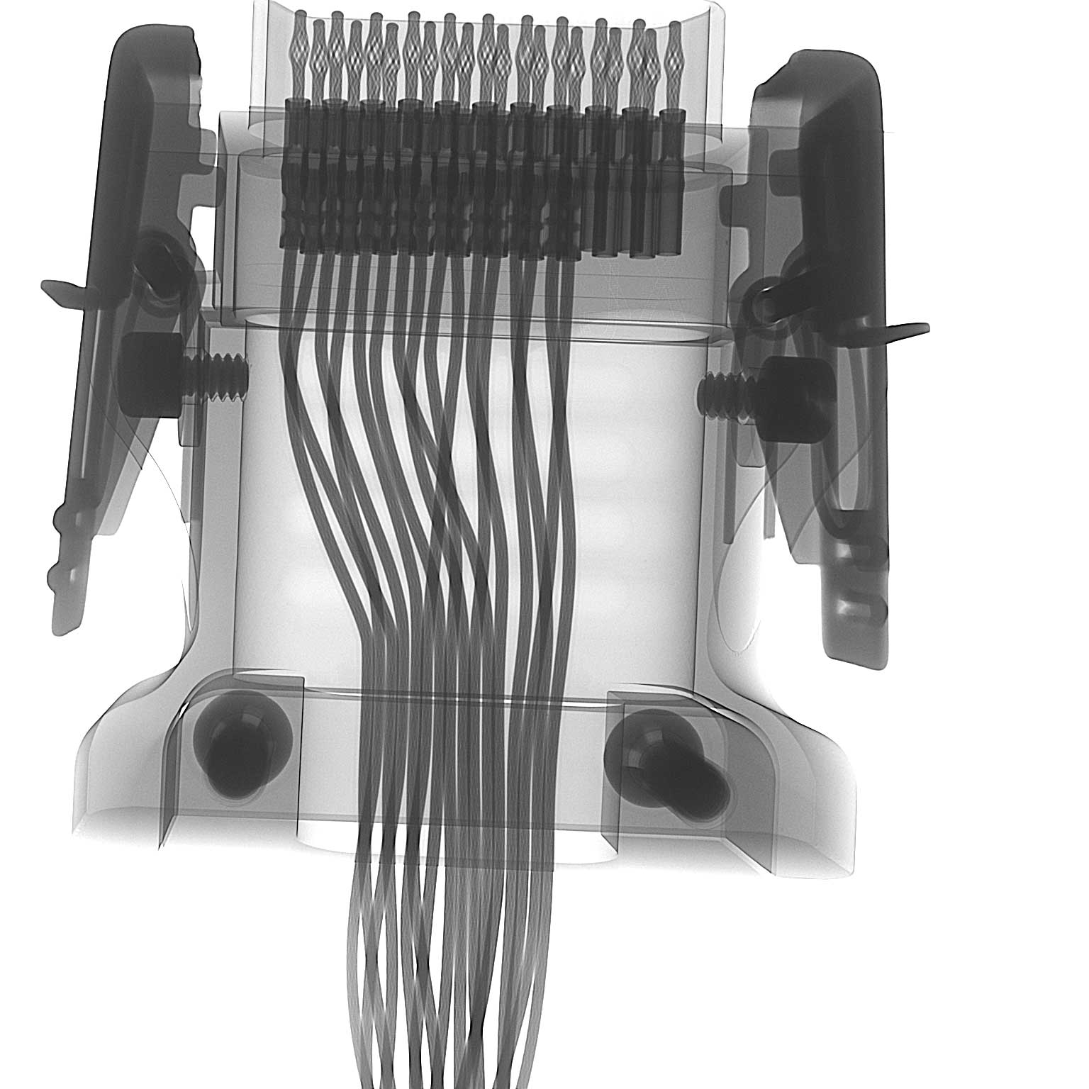
X-Ray NDT for Wire Harnesses & Connectors: Stable QC
In the manufacturing of wire harnesses, cables, and connectors, many defects that affect product reliability are hidden within the internal structure. Traditional visual inspection cannot observe these internal conditions, while destructive cross-sectioning fails to meet the demands for efficiency and mass quality management. Industrial X-Ray inspection technology utilizes high-penetration imaging to perform high-definition internal analysis of key areas—such as conductors, crimps, soldering, pins, injection molding, and insulation—without damaging the product, achieving true non-destructive testing (NDT).
View More
2026-05-15

Uncover Hidden Risks, Protect Value and Reputation — Wahfei Honors Every Hard Worker | Happy Labor Day
Inline full automatic x-ray nspection equipment manufacturer wahfei technology empowering smart manufacturing honoring craftsmanship spirit
View More
2026-04-29
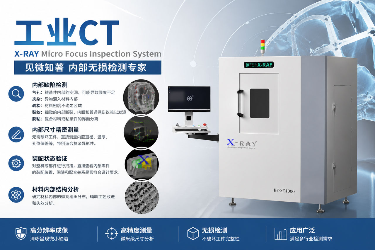
Industrial CT Selection Guide: How to Understand Key Specifications and Choose the Right NDT Equipment?
Compared to other traditional nondestructive testing methods, the greatest advantage of industrial CT is that the images it produces are free from interference caused by overlapping internal structures. This means it can do much more than just "look inside"—it addresses the following in-depth challenges:Unrestricted defect detection from all angles-Destructive-free internal measurement-Assembly integrity verification — inspecting the positioning and engagement of internal components without disassembling the entire machine or sealed parts
View More
2026-04-25
Core Value of X-Ray Inspection for Auto Electronics Suppliers | Fuel Pump Control Module Case
The newly introduced industrial X-ray inspection system uses penetrating X-rays to perform non-contact imaging of the control module, clearly revealing the internal structure of every BGA solder ball and every through-hole solder joint. This means the starting point of quality control has shifted from final electrical verification to the moment the internal structures are formed.
View More
2026-04-23

Actual Video Footage of X-Ray Inline Inspection of SMT Mounting
For FPC flexible boards with multi-area, large-area wiring and micro-SMT components, Inline X-Ray equipment can automatically move the inspection platform (X/Y axes) or adjust the X-Ray tube angle through preset CNC inspection programs to implement comprehensive inspection of different key areas (ROI) on the flexible board without blind spots.
View More
2026-04-17
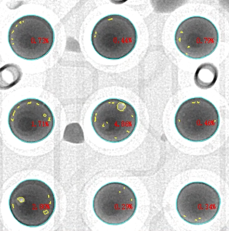
BGA X-Ray inspection technology and quantitative analysis of void defects
leveraging advanced x-ray fluoroscopic imaging technology combined with intelligent image algorithms, we transform the previously “blind-box-like” bga soldering quality—undetectable by the naked eye and conventional instruments—into clearly visible and precisely quantified reports. this not only helps manufacturers quickly intercept defective products from entering the market, but also enables reverse tracking of void ratio trends to guide continuous optimization of front-end smt placement machines and reflow soldering process parameters, thereby improving yield at the source and establishing a solid quality safeguard for the long-term reliability of customer products.
View More
2026-03-31
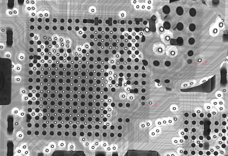
How X-ray inspection systems achieve real-time, non-destructive, and clear imaging of BGA solder joints to ensure soldering quality
In consumer electronics, automotive electronics, and communication equipment, BGA (Ball Grid Array) has become a mainstream packaging method due to its high interconnect density and excellent electrical and thermal performance. However, BGA solder balls are completely hidden beneath the package, making them inaccessible to visual inspection and AOI. X-ray inspection systems utilize X-ray penetration to provide real-time, non-destructive, and clear visualization of internal BGA solder joints, making them essential for ensuring soldering quality. Wahfei’s self-developed X-ray inspection equipment, featuring ultra-high resolution and advanced image processing, delivers precise and reliable solutions for BGA inspection.
View More
2026-03-24