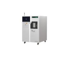
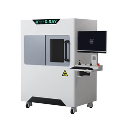
Automated X-Ray Detection of Internal Defects in BGA and IGBT Assemblies
Still chasing solder defects you cannot see? Whether the part is a precision module, a BGA package, or a high-power IGBT, this digital X-ray imaging system identifies internal defects automatically, and takes the strain, the slow throughput, and the missed calls out of manual inspection.
1. Automated Module Inspection: Fast, Accurate, Consistent
The system ships with an extensive library of models built from measured production data, in effect an experienced inspector's eye inside the machine. Model changeover is a single click, and whether the defect is incomplete solder coverage, voids, or stray solder balls, a result comes back within seconds. Even on parts with complex, noisy backgrounds, the AI locates the solder joint region reliably and keeps false calls to a minimum.
2. Void Detection That Holds Up on Any Background
Many conventional X-ray systems misjudge voids when the background tone is uneven. Our intelligent blob detection is built for exactly that condition. Through image preprocessing it adjusts clarity automatically, so voids hidden inside the part are still picked up whether the background is dark or light. On an automated line this is what makes the difference: every image produces a stable result.
3. BGA Inspection That Learns the Layout by Itself
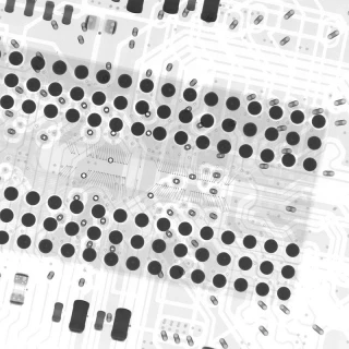
Setting up a BGA inspection used to mean a technician teaching every solder ball position by hand, one at a time. This system offers a self-learning mode: place the sample and it records the ball array automatically. From there it detects missing solder, cold joints, and solder overflow, cutting the engineering workload substantially and putting routine inspection within reach of an ordinary operator.
4. IGBT Defects: Penetration Enough to See Both Layers
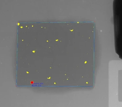
IGBT modules are thick, and conventional systems often cannot see through them. Wahfei X-ray systems use a high-power X-ray source that penetrates the thick copper base plate, resolving both the die-attach solder layer and the DBC solder layer in a single view. Both layers' void percentages are calculated at the same time.
Why Choose Wahfei
Built to resist interference. Complex backgrounds do not affect measurement accuracy.
MES integration. The system connects directly to your factory MES for fully automated in-line inspection.
Efficient by design. A single exposure returns several measurements at once, so line speed is not compromised.
Not sure whether X-ray inspection suits your part or process?
Send us a sample and we will image it on our equipment, then return the results with the measurements that matter for your application. Sample testing is free of charge.
Shenzhen Wahfei Technology Co.,Ltd. designs and manufactures industrial X-ray inspection equipment for electronics manufacturing, semiconductor packaging, power modules, lithium batteries, and other demanding applications.
Values shown in the images are examples from specific samples. Inspection results depend on part geometry, material, and inspection parameters.
WhatsApp +86 189 0297 8624 | szwahfei@gmail.com | www.szwahfei.cn