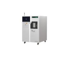
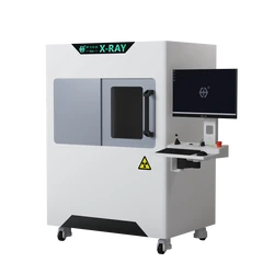
Automated Optical Inspection Machine: Where Surface Checks Need X-Ray Support
An automated optical inspection machine uses cameras, controlled lighting, and image analysis to check visible features on a printed circuit board assembly. Depending on its configuration and inspection program, it can identify missing or shifted components, incorrect orientation where visible markings allow verification, and anomalies in accessible solder joints. Its evidence depends on what the optical system can see.
A clear surface image leaves some questions open
BGA solder joints sit beneath the package body. A component can appear correctly positioned from above while its hidden connections still require inspection. Optical height measurements can improve the assessment of visible geometry, but they do not reveal the internal volume of an opaque solder joint.
X-ray imaging adds information about structures along the beam path. Suitable images may show solder bridges, missing solder balls, and internal voids. Overlapping features and limited contrast can make interpretation difficult, so an additional angle or a suitable sectional imaging method may be needed. A clean-looking image alone does not prove electrical continuity or joint strength.
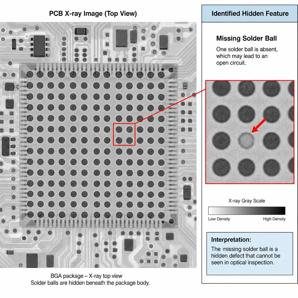
PCB X-ray image showing a clearly identified hidden solder-joint feature.
Build coverage around the remaining risk
Keep optical inspection focused on visible assembly conditions, then select X-ray checks for hidden features that matter to product quality. Electrical testing provides separate evidence of circuit behavior. Shenzhen Wahfei Technology Co.,Ltd. manufactures industrial X-ray inspection equipment; AOI equipment is a separate product category. Discuss the sample structure and target defect with Wahfei Technology to assess the appropriate X-ray inspection approach.