


BGA X-Ray inspection technology and quantitative analysis of void defects
- Pubdate 2026-03-31
X-ray inspection of bga solder joints
bga (ball grid array) has become a mainstream high-density packaging technology. its core advantage lies in that the chip pins are distributed as spherical or columnar solder balls in an array on the bottom of the chip, greatly saving pcb space. however, this design also brings a critical quality control challenge: after soldering onto the circuit board, the solder joints are completely hidden and invisible, making traditional optical inspection (aoi) ineffective. to ensure absolute reliability of electronic products, introducing high-precision micro-focus x-ray inspection equipment has become an inevitable choice for enterprises.
1. hidden threats: common defects and causes of voids in bga solder joints
in actual production, common soldering defects of bga joints include voids, insufficient soldering, cold solder joints, oversized solder joints, and bridging short circuits. among them, voiding defects are the most common and highly concealed.
the formation of voids is mainly due to the rapid vaporization of organic substances (flux) in the solder under the high temperature of reflow soldering. these gases are trapped inside the molten liquid solder and solidify before escaping. these tiny bubbles should not be underestimated, as they interrupt the internal metal continuity of the solder joint, resulting in reduced mechanical strength, decreased thermal conductivity, and impaired high-frequency signal transmission. under long-term operation or vibration conditions, voids can easily induce microcracks, ultimately leading to complete product failure.
2. strict quality control: industry inspection standards for bga void defects
due to physical limitations, completely eliminating voids is unrealistic. therefore, industry standards (such as ipc standards) allow a certain size of micro voids inside solder balls, but impose extremely strict limits on the void ratio. precise control of the void ratio is the key factor in determining whether a product can be shipped:
it can be seen that the core technical challenge and key point of detecting bga void defects lies in how to accurately penetrate the chip and precisely calculate the ratio between the "void area" and the "solder ball area" with high precision.
3. see through everything: nondestructive x-ray imaging principle for bga solder joints
when performing high-quality inspection of bga packaged devices, the x-ray source inside the equipment emits high-energy radiation. after penetrating the pcba with complex circuits and components, the rays are absorbed differently depending on material density. the unabsorbed rays are precisely captured by the image intensifier or flat panel detector below and ultimately converted into grayscale digital images with clear contrast.
here, a key hardware parameter determines the inspection capability: the focal spot size of the x-ray source. the smaller the focal spot (micron or even nanometer level), the closer the emission source is to a point source, resulting in sharper image edges, higher geometric accuracy, and greater sensitivity—making even micro voids as small as a fraction of a hair detectable.
the image below shows the inspection of a plastic-encapsulated bga chip soldered by reflow under a high-end x-ray system. in the localized high-definition image, the solder ball morphology hidden beneath the chip is fully revealed. circular bubbles (voids) formed due to poor outgassing inside the solder balls are clearly visible, with strong black-and-white contrast.
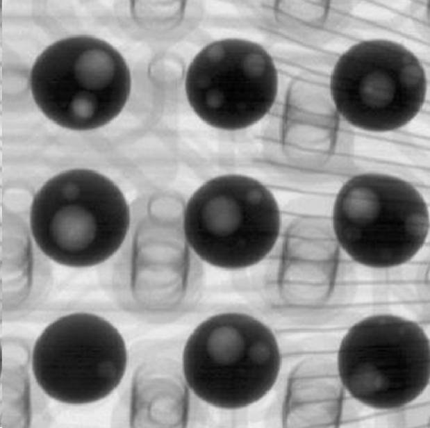
figure 1: clearly visible bubble (void) morphology inside bga solder joints
4. data-driven quality control: intelligent quantitative analysis of bga void defects
merely observing voids is not enough; modern intelligent inspection emphasizes data quantification. professional inspection systems are equipped with advanced image processing algorithms capable of automatic segmentation, extraction, and computation of acquired bga images.
taking the 9 representative bga solder joints in figure 1 as an example, the system first performs contour recognition. as shown below, each bga solder joint is precisely segmented and extracted by the algorithm. meanwhile, using grayscale threshold analysis, the system accurately extracts the brighter regions within the solder joints (areas with higher x-ray transmission and lower density, i.e., void defects) and highlights them with special colors on the original image. in addition, the system automatically numbers the solder joints in sequence by column coordinates (e.g., 1–9), ensuring no missed inspections or misjudgments.
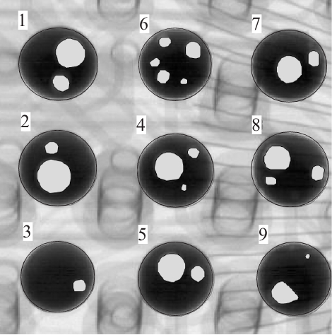
figure 2: automatically segmented bga solder joints and highlighted internal void regions
after successful contour extraction, the system enters a high-speed pixel-level computation stage. it calculates the total pixel count of the bga solder joint and the pixel count of the internal void regions. based on pixel equivalence, the system converts these into the "equivalent total area of the bga solder joint" and the "equivalent void area", and finally automatically generates a precise area ratio (void ratio) analysis report.
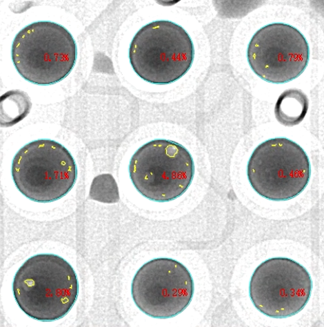
figure 3: example of automatically generated quantitative bga void ratio results
leveraging advanced x-ray fluoroscopic imaging technology combined with intelligent image algorithms, we transform the previously “blind-box-like” bga soldering quality—undetectable by the naked eye and conventional instruments—into clearly visible and precisely quantified reports. this not only helps manufacturers quickly intercept defective products from entering the market, but also enables reverse tracking of void ratio trends to guide continuous optimization of front-end smt placement machines and reflow soldering process parameters, thereby improving yield at the source and establishing a solid quality safeguard for the long-term reliability of customer products.