


How X-ray inspection systems achieve real-time, non-destructive, and clear imaging of BGA solder joints to ensure soldering quality
- Pubdate 2026-03-24
BGA solder joints invisible? Use X-Ray inspection system to penetrate the chip and accurately inspect each solder ball.
In fields such as consumer electronics, automotive electronics, and communication equipment, BGA (Ball Grid Array) has become the mainstream chip packaging method due to its high-density interconnect and excellent electrical and thermal performance. However, BGA solder balls are completely hidden beneath the package body, making them inaccessible to traditional visual inspection and AOI optical inspection. X-Ray inspection systems utilize the penetrating properties of X-rays to present the internal state of BGA solder balls in real-time, non-destructively, and with high clarity, making them an indispensable core inspection equipment for ensuring BGA soldering quality. The X-Ray inspection equipment independently developed by Huafei Technology provides an accurate and reliable solution for BGA inspection with ultra-high resolution and a versatile image processing system.
Article Navigation
I. What is BGA Packaging? Why Can't Traditional Methods Inspect It?
II. Core Principle of X-Ray Inspection for BGA Solder Joints
III. What BGA Solder Joint Defects Can X-Ray Detect?
IV. BGA X-Ray Inspection Actual Effect Display
V. Huafei HF-S90 6-Axis X-Ray Equipment Specifications
What is BGA Packaging? Why Can't Traditional Inspection Methods See BGA Solder Joints?
BGA is an advanced packaging technology that arranges the input/output pins of an integrated circuit in the form of solder ball arrays uniformly on the bottom of the package. Unlike traditional QFP or SOP packaging, BGA pins are not exposed around the package but are hidden directly beneath the chip as tiny solder balls. A typical BGA chip may contain hundreds or even thousands of solder balls, with a minimum pitch of 0.3mm.
While this high-density structure offers excellent electrical and thermal performance, it also presents significant challenges for soldering quality inspection:
Solder joints completely invisible —— BGA solder balls are completely obscured by the package body, making direct observation impossible from any angle.
AOI inspection ineffective —— Automatic optical inspection can only check component appearance and placement position, unable to penetrate the package body.
Manual visual inspection unreliable —— Even with high-power microscopes, the BGA bottom solder joint condition cannot be observed.
Destructive testing costly —— Cross-section analysis is accurate but destroys the product, only suitable for sampling verification.
Therefore, the recognized best solution in the electronics manufacturing industry is to use X-Ray inspection systems for non-destructive inspection of BGA solder joints – it is currently the only technical means to comprehensively inspect BGA soldering quality without damaging the product.
Core Principle of X-Ray Inspection for BGA Solder Joints
The working principle of the X-Ray inspection system is based on the penetration and differential absorption characteristics of X-rays. The X-ray tube generates a high-energy beam that penetrates the BGA component being inspected and is received by a high-precision flat panel detector, converting it into a real-time digital image. Different materials have significantly different absorption rates for X-rays, which is the physical foundation for BGA inspection:
Solder Ball Material (Tin/Lead/Silver/Copper)
High X-Ray Absorption
Appears as dark, high-contrast areas in the image
PCB Substrate & Packaging Materials
Low X-Ray Absorption
Appears as light, low-contrast areas in the image
This natural grayscale contrast makes BGA solder balls clearly distinguishable in X-Ray images. Inspection engineers evaluate soldering quality comprehensively by analyzing the following key parameters:
01
Solder Ball Shape
02
Solder Ball Size
03
Solder Ball Position
04
Internal Voids
05
Solder Ball Pitch
06
Grayscale Value Analysis
What BGA Solder Joint Defects Can X-Ray Inspection Systems Detect?
Below are the six most common types of defects in BGA soldering, all of which can be accurately identified and quantitatively analyzed by X-Ray inspection systems:
BGA Solder Joint X-Ray Inspection Actual Effect Display
The image below shows the actual inspection result of a BGA component using Huafei Technology's X-Ray inspection equipment. The BGA ball array, via solder joints, and internal PCB trace structure are clearly visible. The shape, size, and distribution of the balls are evident at a glance, providing an intuitive and reliable basis for soldering quality assessment.
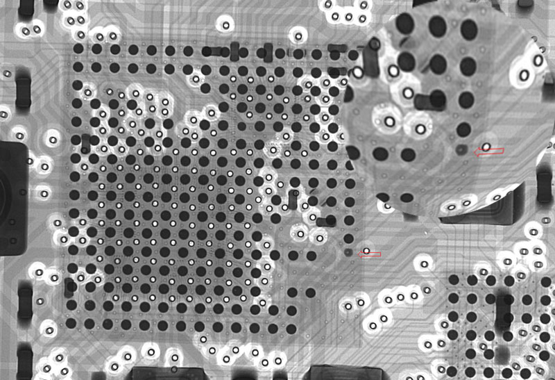
Actual X-Ray Inspection Image of BGA Solder Joints —— Captured by Huafei Technology HF-S90
Huafei Technology HF-S90 6-Axis X-Ray Inspection Equipment —— A Reliable Choice for BGA Inspection
Huafei Technology's HF-S90 is a 6-axis multifunctional X-Ray inspection system designed specifically for high-precision electronic inspection. It is widely used for BGA solder joint inspection in SMT, DIP assembly processes, semiconductor IC packaging, new energy lithium batteries, capacitor components, automotive parts, and other fields. The core specifications are as follows:
Core Highlights: The proprietary X-Mind multifunctional image processing system ensures X-Ray inspection results are free from distortion, energy loss, or compressed inspection range. Combined with the 6-axis control system, it allows flexible observation of BGA solder joints from multiple angles and dimensions. Paired with the 5μm ultra-high resolution flat panel detector, even tiny voids and fine bridging are unmistakably revealed.
Core Advantages of Choosing Huafei Technology for BGA X-Ray Inspection
BGA X-Ray Inspection Frequently Asked Questions
Q: Can X-Ray inspection damage the BGA product?
A: No. X-Ray inspection is a Non-Destructive Testing (NDT) technique. The X-ray energy levels used do not cause any physical damage to electronic components, PCBs, or solder joints. Inspected products can be used and shipped normally. This is a core advantage of X-Ray compared to destructive methods like cross-sectioning.
Q: What is the acceptable BGA void percentage? Can X-Ray measure it accurately?
A: According to IPC-7095 (Guidelines for BGA Design and Assembly Process Implementation) and IPC-A-610 standards, the void area percentage in BGA solder joints is typically required to not exceed 25%. The Huafei HF-S90, equipped with the X-Mind image processing system, can accurately calculate the void area percentage for each ball, providing quantitative inspection data that meets quality control and customer audit requirements.
Q: My BGA pitch is very small (below 0.4mm). Can the HF-S90 see it clearly?
A: Yes. The HF-S90 is equipped with a 600mm x 600mm flat panel detector featuring 5μm resolution. It can clearly resolve BGA balls with a pitch of 0.3mm or even smaller. Combined with the magnification and tilt capabilities of the 6-axis control system, high-quality inspection images can be obtained even for ultra-fine pitch BGAs.
Q: Can I test samples before deciding to purchase the equipment?
A: Certainly. Huafei Technology offers a free sample testing service. You can simply send your BGA samples to our laboratory in Guangming District, Shenzhen. Our engineers will perform the actual inspection using the HF-S90 and provide a comprehensive inspection report and images, helping you evaluate the equipment's performance visually.
Unsure if an X-Ray Inspection System meets your BGA inspection needs?
Huafei Technology offers a free sample testing service. Let real inspection results speak for themselves. Contact us today for a customized BGA X-Ray inspection solution and quote.
Contact Us NowNational Service Hotline: 400-728-7288 | 18902978624 (WeChat)