


3D-CT AXI Enables Non-Destructive Testing of IGBT Power Modules
- Pubdate 2026-02-07
3D-CT AXI Inspection of IGBT Power Modules
High-Speed, High-Precision 3D-CT AXI Solution
In the semiconductor industry, the reliability of IGBT (Insulated Gate Bipolar Transistor) power modules is critical. Internal defects such as voids within solder layers are key hidden risks that directly affect performance and service life. To address this challenge, Wahfei has introduced a 3D-CT AXI inspection system specifically designed for IGBT power modules. While achieving industry-leading inspection speed, the system reliably detects manufacturing defects that are difficult to identify using conventional methods, and also offers excellent ease of operation and maintainability.
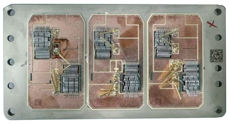
IGBT power module awaiting inspection
Core Advantage: Superior Void Detection Enabled by Planar CT Technology
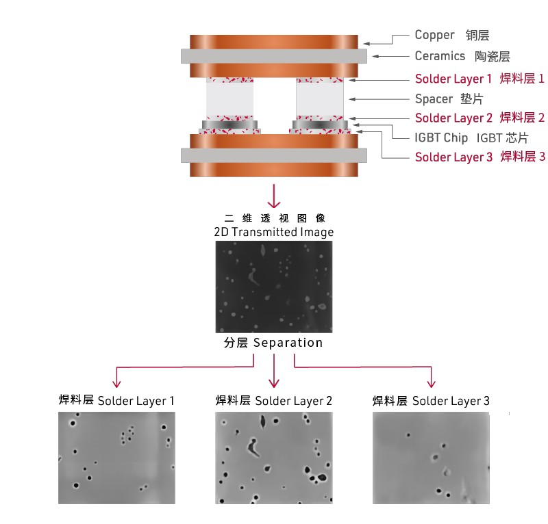
In conventional 2D X-ray inspection, vertical X-ray penetration causes overlapping images of heat sinks, spacers, and multiple solder layers, making it impossible to accurately measure voids within an individual solder layer.
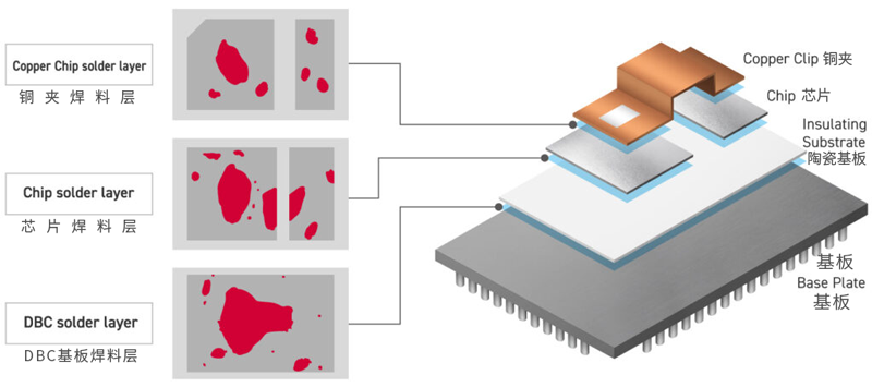
Cross-sectional diagram of an IGBT power module
Wahfei’s 3D-CT AXI inspection system adopts a unique Planar CT imaging technology, optimized specifically for flat-structured components. This technology clearly separates each individual solder layer, enabling precise identification and measurement of hidden micro-voids, and achieving true 3D non-destructive inspection.
Stable and Reliable Imaging Driven by Precision Hardware Design
Outstanding inspection performance is built upon a solid hardware foundation. The system features a high-rigidity frame and high-precision linear scales to ensure accurate positioning and stable imaging. During image reconstruction, platform position data is calibrated in real time, ultimately generating high-definition tomographic images with sharp edges and rich details, providing a reliable basis for accurate defect evaluation.
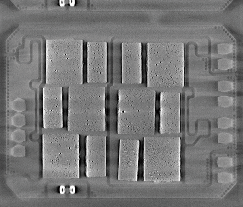
IGBT solder layer void inspection result image 1
Intelligent Algorithms for Accurate OK/NG Judgment
Benefiting from a high-power X-ray source, the system is particularly suitable for inspecting thick and heavy power modules. It can effectively penetrate high-density materials such as heat sinks, remain unaffected by their noise, and reliably identify void defects.
The innovative void detection algorithm integrates advanced noise-reduction filters, enabling accurate recognition of micro-voids that were previously difficult to distinguish. As shown, the algorithm effectively suppresses artifacts, more precisely restores defect conditions, and automatically determines product acceptance or rejection (OK/NG) based on these results.
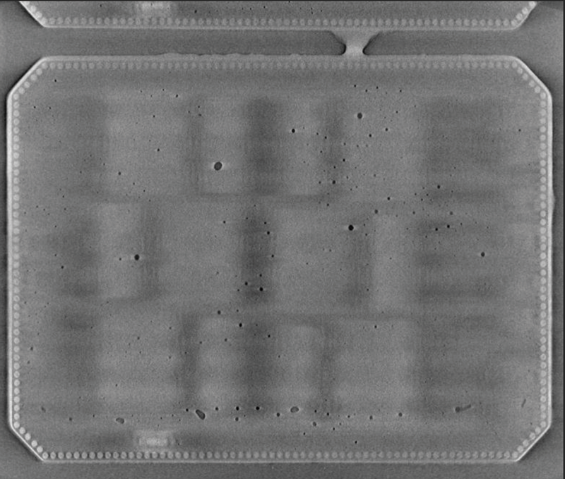
IGBT solder layer void inspection result image 2
Broad Compatibility for Thin DSC Power Modules
With ongoing technological advancement, thin and lightweight DSC (Discrete and System Components) power modules are becoming increasingly common. Even when faced with these components featuring more layers and more compact structures, the 3D-CT AXI inspection system can clearly separate spacers and individual solder layers, accurately capturing void defects.
Cross-sectional view of a DSC power module
Improving Production Efficiency and Equipment Maintainability
1. Offline Debugging Without Production Interruption
The unique offline debugging function allows engineers to analyze and fine-tune previously captured defect images without stopping the production line. Algorithm library updates can be completed in real time without system downtime. In addition, the storage and review of historical defect data provide strong support for quality assurance and ongoing algorithm optimization.
2. Long-Life Hardware and Intelligent Self-Diagnostics
High-durability design: In high-volume production environments, the system must maintain long-term precision and stability. By adopting a proprietary high-rigidity frame and easily replaceable modular design, the equipment lifespan is extended and maintenance procedures are greatly simplified. At the same time, the optimized lead shielding design for the detector significantly reduces radiation-induced sensor degradation.
Extended self-diagnostic functions: To ensure consistently high-precision inspection, the system periodically performs self-diagnostics on key parameters such as X-ray source status, image uniformity, and image distortion. This enables planned maintenance, effectively prevents unexpected failures, reduces downtime, and avoids unnecessary spare part replacement, thereby lowering overall operating costs.