


The Mandatory Final Check: X-Ray for Zero-Defect PCBA Manufacturing
- Pubdate 2026-01-16
Tectec Technology (Shenzhen) Deploys X-Ray Inspection System to Enhance PCBA Motherboard Quality
Tectec Technology (Shenzhen) Co., Ltd. was established in May 2018, boasting a 2,000 square meter office and production facility with an excellent environment and convenient transportation. The company's headquarters, Antai Technology (Beijing) Co., Ltd., is located in Haidian District, Beijing.
As a high-tech enterprise integrating independent R&D, production, system integration, sales, and service, Tectec Technology specializes in motherboard and complete system solutions for industrial computers, network security computers, servers, and industrial control equipment. The company has established a comprehensive customized service system covering early-stage design, small-batch verification, mass production, after-sales maintenance, technical support, and on-site service. It possesses core manufacturing capabilities including PCBA SMT production lines and sheet metal chassis production lines. Based on the X86 technology platform, its products are widely used in firewalls, UTM, IDS/IPS, encryptors, network load balancers, Internet behavior management, physical isolation, and intranet security. Tectec Technology has passed ISO9001 quality system certification and is recognized as a National High-Tech Enterprise. Its R&D team possesses over a decade of industry experience, and its products hold multiple patents. The company maintains close cooperative relationships with several internationally leading manufacturers.
X-Ray: The Mandatory Final Check Before Product Delivery
Tectec's products extensively utilize high-density BGA package chips and multi-layer PCB designs. For such components, the solder joints are completely hidden beneath the chip, making them inaccessible to traditional inspection methods. Taking a typical network processor BGA as an example, hundreds of solder balls may be densely packed underneath. Any issues like voids, cold joints, or bridging in a single ball can potentially evolve into intermittent failures during long-term operation. Such faults are extremely difficult to diagnose and often only manifest after the equipment is deployed at the customer site, leading to incalculable repair costs and brand damage.
X-Ray inspection technology can penetrate the chip package, directly revealing the internal structure of the solder joints. Critical information such as whether voiding exceeds standards, if solder balls exhibit complete wetting, or if there is any short circuit between adjacent joints becomes immediately clear in the X-ray image. For manufacturers pursuing zero-defect delivery, this is not an option but a mandatory final checkpoint before product shipment.
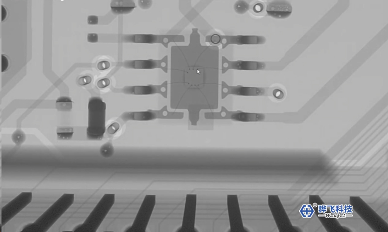
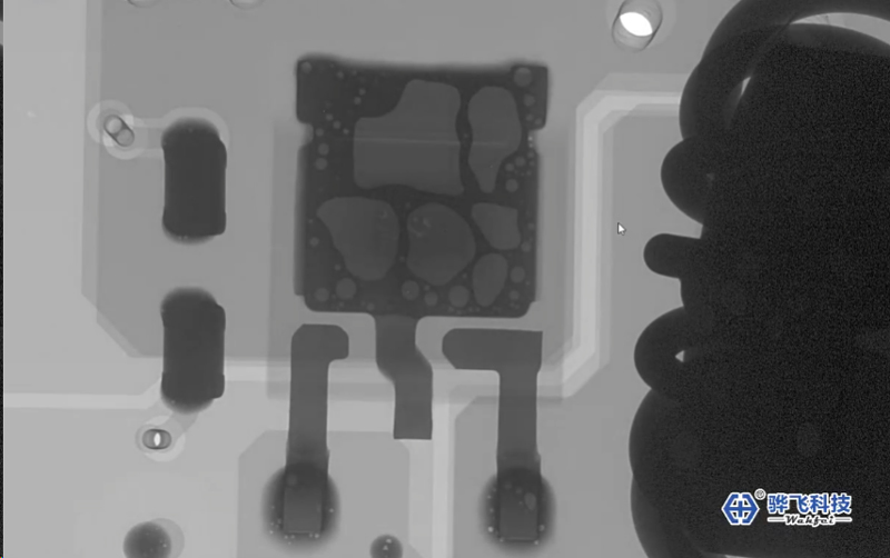
In accordance with commercial information agreements and respect for intellectual property, the X-ray inspection images displayed here are for technical capability demonstration only.
Wahfei sincerely invites you to provide or bring/mail samples to obtain relevant inspection reports free of charge.
To learn how X-Ray inspection equipment can empower your SMT production line
Please feel free to call for consultation or schedule a free sample inspection service.