


X-Ray Inspection System Applications in Various Industrial Products
- Pubdate 2026-01-17
X-RAY Application Analysis
In high-end manufacturing and precision electronics industries,
X-Ray Inspection Systems have become indispensable quality control tools.
Compared with traditional visual inspection, cross-sectioning, or destructive testing methods,
X-Ray technology enables direct visualization of the internal condition of products
without damaging the sample structure,
and is widely applied in power devices, electronic packaging, new energy, and advanced materials.
The following sections combine real inspection images to systematically analyze X-Ray inspection priorities,
detectable defect types, and their engineering value across different products,
providing reference for R&D, quality, procurement, and technical decision-makers.
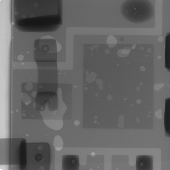
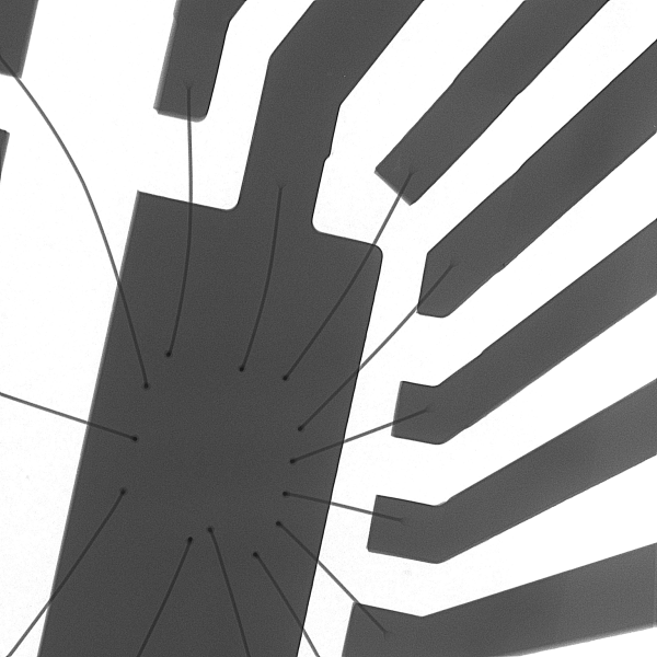
IGBT Module X-RAY Non-Destructive Inspection
As a core component of power electronics, the internal solder layers and chip interconnection reliability of
IGBTs
directly determine the service life of the entire system.
X-Ray imaging clearly reveals solder uniformity, void ratio, cracks, and wire bonding conditions.
Detectable defects: solder voids, uneven solder layers, chip misalignment, internal cracks
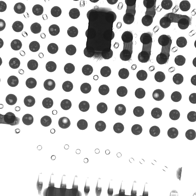
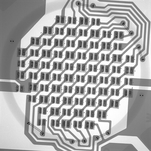
PCBA / BGA Solder Joint X-RAY Inspection
For invisible solder joints such as
BGA
and QFN packages, X-Ray is the only method capable of quantitative solder quality analysis,
widely used for in-line sampling inspection and failure analysis.
Detectable defects: cold solder joints, solder bridging, solder ball voids, joint misalignment
LED Headlight Structure X-RAY Inspection
X-Ray can penetrate metal housings to directly observe the internal chip layout, soldering,
and thermal structures of
LED
modules, which is critical for reliability evaluation.
Detectable defects: chip misplacement, abnormal soldering, internal structural defects
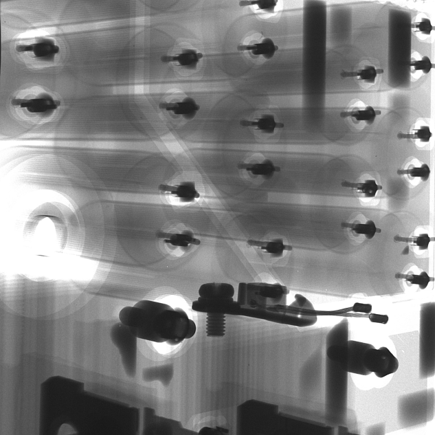
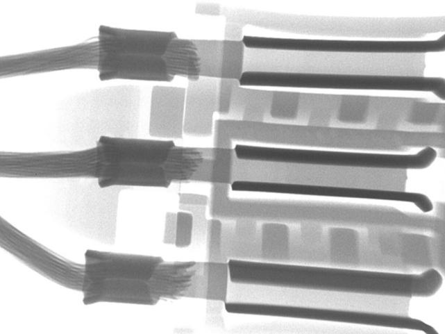
Connector / Plug X-RAY Inspection
Due to the complex internal terminal structures of
connectors,
X-Ray enables intuitive evaluation of terminal forming, crimping depth, and internal misalignment.
Detectable defects: terminal misalignment, poor crimping, internal fractures
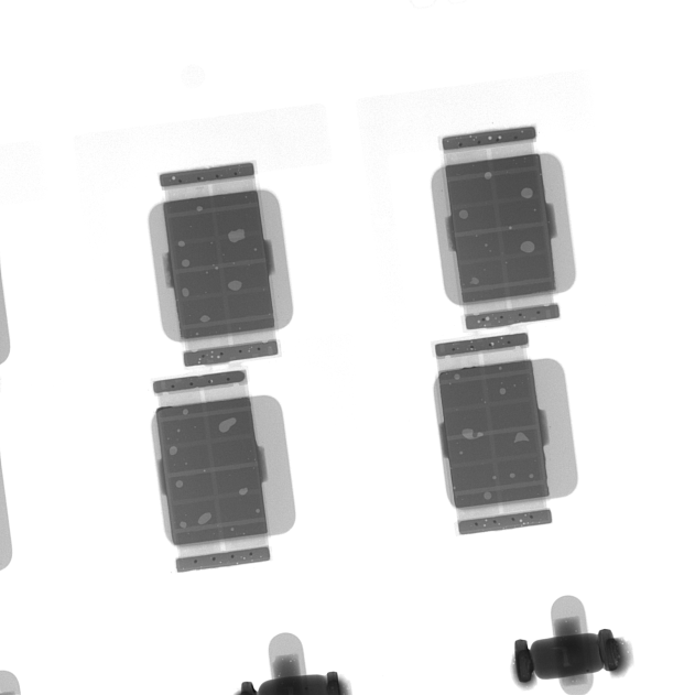
Semiconductor Package X-RAY Inspection
X-Ray is a core method for
evaluating internal solder joints and structural integrity .
Detectable defects: package voids, abnormal wire bonding, chip misalignment

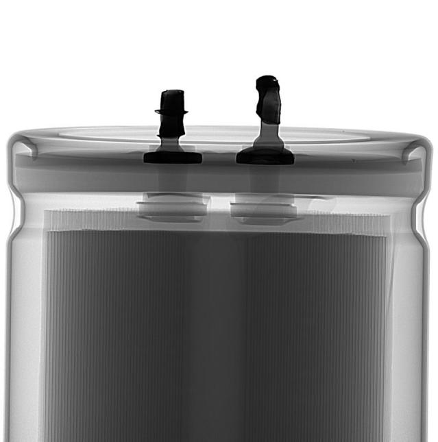
Lithium Battery X-RAY Non-Destructive Inspection
X-Ray is used to observe cell winding, electrode alignment, and internal foreign objects,
making it an essential tool for new energy battery safety inspection.
Detectable defects: electrode misalignment, internal foreign matter, structural deformation
Capacitor X-RAY Inspection
Enables observation of internal electrode arrangement, soldering quality,
and package integrity, suitable for failure analysis and reliability validation.
Detectable defects: abnormal internal structure, poor soldering
Wire / Bond Wire X-RAY Inspection
For fine wires and bonding structures, X-Ray can identify internal breaks
or abnormal routing invisible to the naked eye.
Detectable defects: wire breakage, internal displacement, structural abnormalities
LED / Diamond X-RAY Inspection
For high-density or high-value materials, X-Ray is used to detect internal defects,
cracks, and structural consistency.
Detectable defects: internal cracks, structural non-uniformity, inclusions
As manufacturing precision continues to increase, traditional inspection methods can no longer meet
high reliability requirements.
X-Ray inspection systems are gradually evolving from “problem analysis tools”
to “process quality assurance tools,”
playing an increasingly critical role in R&D validation, production sampling,
and failure analysis.