


X-Ray Automated Inspection for Internal Product Defects - Solving Inspection Challenges for BGAs, IGBTs
- Pubdate 2026-01-15
Struggling with invisible soldering defects?Whether your products are precision modules, BGA chips, or high-power IGBTs, thisX-ray digital imagingsystem automatically identifies internal defects, eliminating the pain points of labor-intensive manual inspection, low efficiency, and missed defects.
01. Automated Module Inspection: Fast, Accurate, Reliable
The system comes with a large library of verified inspection models—like giving the equipment the eyes of a seasoned expert. It supports one-click switching between multiple product types. Whether it’s insufficient solder coverage, internal voids, or excess solder balls, results are delivered in seconds. Even for parts with complex backgrounds and heavy interference, AI algorithms precisely lock onto the solder joint area, ensuring stable detection without false alarms.
02. Instant Void Identification Across Complex Backgrounds
Many conventional X-ray systems are prone to misjudgment when background grayscale is uneven. Our “intelligent speckle detection technology” is immune to such interference. Through image preprocessing, the system automatically optimizes image clarity. Regardless of whether the background is dark or bright, hidden voids are captured accurately. This is especially valuable on automated production lines, ensuring consistent and reliable inspection results for every image.
03. Self-Learning BGA Inspection
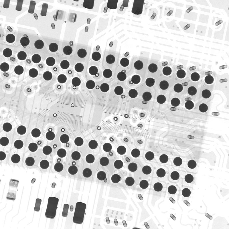
(Image: Automatic recognition of BGA solder ball layout with clearly visible defects)
In the past, configuring BGA inspection required technicians to manually define each position—time-consuming and inefficient. Now, the system features a self-learning mode. Simply place the sample, and it automatically learns and records the solder ball layout. Missing solder, cold joints, and solder overflow are detected automatically, significantly reducing the workload for engineers and allowing even standard operators to handle inspections with ease.
04. IGBT Defect Inspection: Powerful Penetration, Clear Imaging of Dual Layers
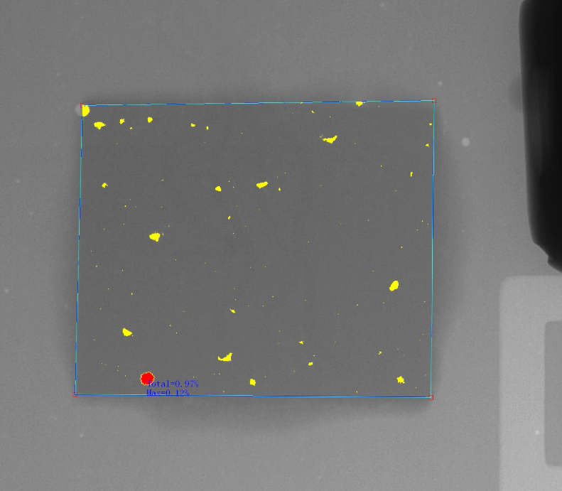
(Image: Clear visualization of voids in both solder layers of an IGBT module)
IGBT modules are thick, making them difficult for standard equipment to penetrate. Wahfei X-Ray uses a high-power X-ray source capable of penetrating thick copper substrates, allowing clear visualization of both the chip solder layer and the DBC solder layer. Most importantly, the system can simultaneously calculate the void ratio for each layer.
Strong anti-interference capability: Accurate results even under complex backgrounds.
System integration: Direct connection with factory MES systems for fully automated online inspection.
High efficiency, worry-free operation: Single image acquisition with multiple data outputs, without slowing down the production line.