


X-Ray CT Inspection of Silicon Carbide Cracks and Inclusions
- Pubdate 2026-01-06
Microscopic Insight: 3D X-Ray CT Non-Destructive Inspection of
Internal Cracks and Inclusions in Silicon Carbide (SiC)
As a core material of third-generation semiconductors, silicon carbide (SiC) is highly prone to generating internal micro-cracks, voids, and inclusions that are invisible to the naked eye during crystal growth and machining. If not eliminated, these defects can cause device failure under high-voltage and high-temperature operating conditions. Industrial-grade X-Ray CT inspection systems leverage tomographic scanning technology to become a key solution to this challenge.
Comparative CT Inspection Images of SiC Samples
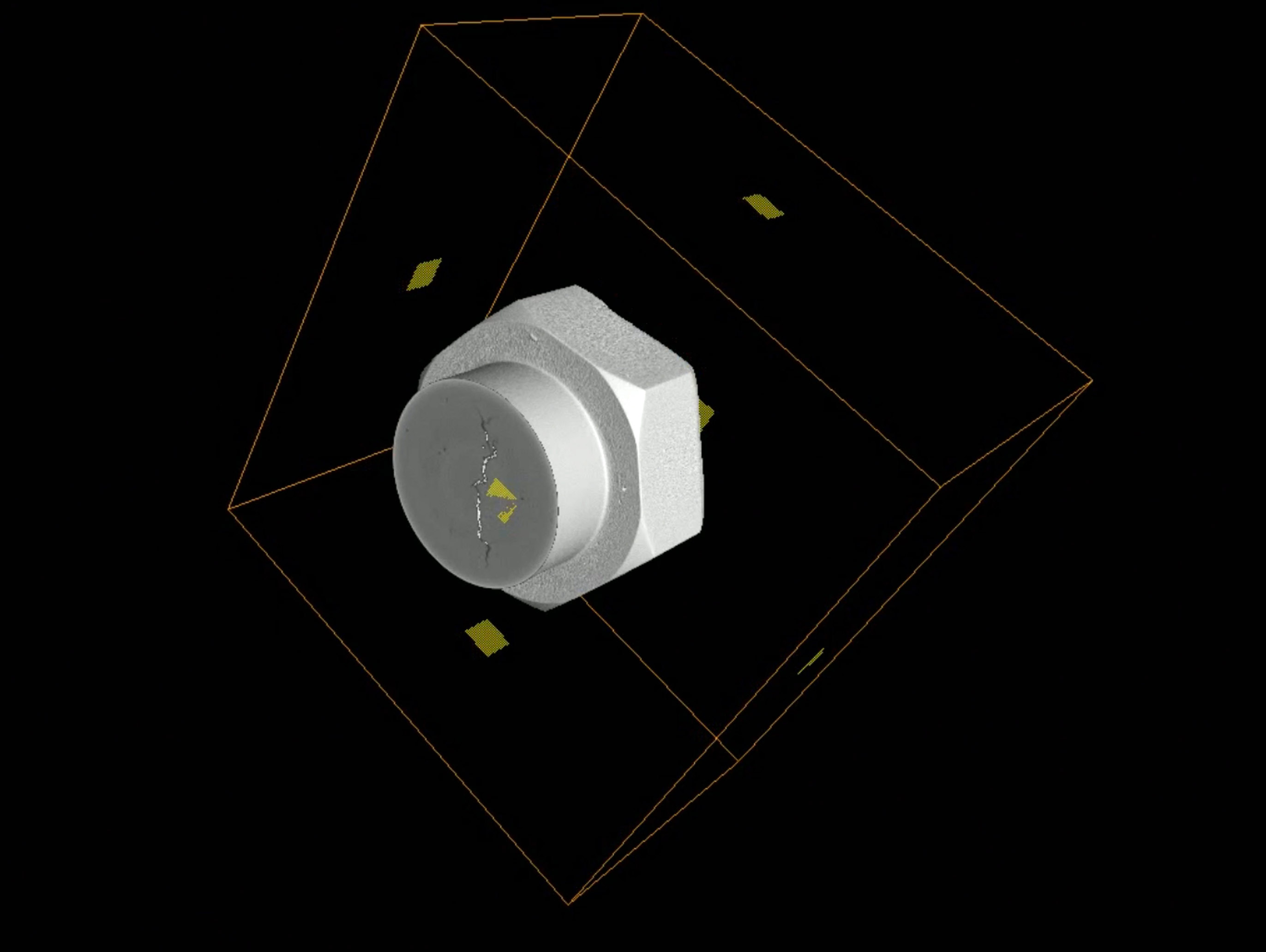
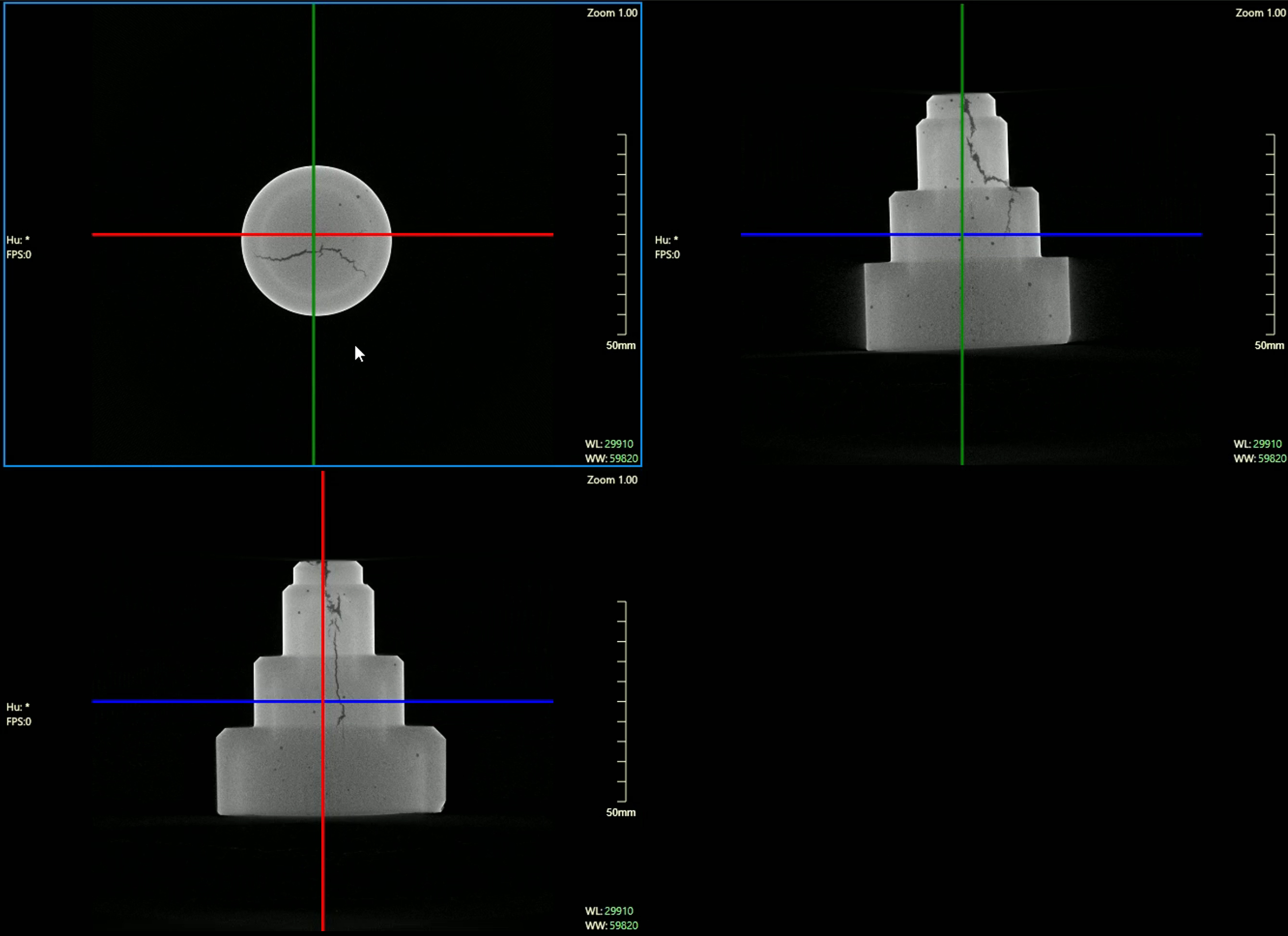
In accordance with commercial confidentiality agreements and respect for intellectual property rights, the X-Ray inspection images shown here are for technical capability demonstration purposes only.
Wahfei sincerely invites you to bring or ship samples to experience the actual inspection performance of the system.