Microfocus X-Ray Inspection System: How It Produces High-Resolution Internal Images
Microfocus X-Ray Inspection System: How It Produces High-Resolution Internal Images
A microfocus x-ray inspection system is designed for products whose important features are small, hidden, or difficult to inspect without cutting the sample open. Its main advantage comes from a very small X-ray focal spot, which reduces geometric blur and supports magnified imaging.
That makes microfocus inspection useful for semiconductor packages, SMT assemblies, BGA joints, batteries, connectors, and other precision parts. The right configuration, however, depends on the sample and the defect the manufacturer needs to find.
Why the focal spot matters
When an X-ray source passes through a part, the detector records differences in X-ray attenuation. Dense materials absorb more X-rays; air gaps and voids absorb less. The result is a grayscale image of the internal structure.
The focal spot is the small area where the electron beam strikes the target. A smaller focal spot behaves more like a point source. It reduces penumbra, or edge blur, and allows the sample to be placed close to the source for geometric magnification. This is the physical reason a microfocus system can reveal small internal features more clearly than a larger-focus source in the same inspection setup.
Focal spot size is not the same as total system resolution. Practical image quality also depends on the detector, sample thickness and material, source-to-object distance, object-to-detector distance, motion stability, image processing, and the inspection recipe. A high magnification number alone does not prove that a system can resolve a particular defect.
What a microfocus system can inspect
Microfocus X-ray inspection is commonly selected when the target contains fine internal structures or concealed joints.
- Semiconductor packages: die, lead frames, bond wires, package voids, and internal alignment.
- SMT and PCBA: BGA and QFN solder joints, hidden bridges, voids, and components under packages.
- Batteries: internal alignment, tabs, weld areas, and selected structural features, subject to the cell design and material thickness.
- Connectors and wire assemblies: terminal position, crimp structure, wire placement, and internal fit.
- Precision parts: small cavities, inclusions, cracks, or assembly relationships that cannot be confirmed from the outside.
The correct application must still be confirmed with representative samples. The material stack-up, part geometry, and required defect size determine whether microfocus 2D imaging is sufficient or whether 3D CT, a different detector, or a higher-energy source is needed.
Microfocus versus conventional-focus inspection
Microfocus and conventional-focus X-ray systems are not simply good and bad versions of the same machine. They are optimized for different inspection problems.
| Feature | Microfocus system | Conventional-focus system |
|---|---|---|
| Main strength | Fine detail and magnified imaging | Penetration and broader coverage |
| Typical target | Electronics, packages, small precision parts | Larger or thicker industrial components |
| Focal spot effect | Lower geometric blur | More geometric blur at high magnification |
| Best question | What is happening inside this small feature? | Is there a significant internal defect in this larger part? |
| Main trade-off | High detail may require careful setup and suitable thickness | Higher power may reduce fine-detail capability |
The comparison is a starting point, not a purchasing rule. Some systems support multiple operating conditions, and the best choice depends on the actual samples and acceptance criteria.
The main parts of the system
The source, detector, motion system, and software work together; the following components determine whether the image is useful.
Microfocus X-ray source
The source determines the available energy and focal-spot conditions. Tube voltage affects penetration and image contrast, while power and thermal management affect operating stability. The source should be evaluated with the material and thickness of the intended samples, not by focal-spot size alone.
Detector
The detector converts the transmitted X-ray pattern into a digital image. Pixel size, active area, dynamic range, contrast response, and noise all influence the usable image. A small focal spot cannot compensate for a detector or setup that does not capture the required detail.
Precision motion and geometry
The source, sample, and detector must remain stable during imaging. Multi-axis motion, rotation, tilt, and accurate positioning help the operator find a useful view of complex assemblies. Geometry is particularly important when magnification is used.
Imaging software
Software supports image enhancement, measurement, recipe management, defect review, and reporting. Automated analysis can help with repeatable inspection, but the algorithm must be validated against known good parts, known defects, and the customer's acceptance rule.
Shielded enclosure and safety interlocks
A cabinet system is designed to contain radiation during normal operation. Door interlocks, shielding, warning systems, and leakage checks are part of safe operation. Operators still need the training and procedures required by applicable local regulations.
What the image can add to electrical test
Electrical test answers whether a circuit or device behaves within its specified limits. X-ray answers whether hidden physical structures are present and assembled as intended. The two methods provide different evidence.
A connector can show continuity while the terminal is not seated at the intended position. A solder joint can conduct while containing a void or having poor internal coverage. A semiconductor package can pass an electrical test while its internal construction still requires investigation. X-ray does not replace electrical testing; it helps explain the physical causes behind process drift, intermittent failures, and reliability concerns.
For production, the inspection plan may use inline X-ray for automated coverage, offline microfocus inspection for engineering and failure analysis, or a combination of both. The appropriate arrangement depends on volume, cycle time, product risk, and the cost of a missed defect.
Example: HF-S160 open-tube microfocus X-ray system
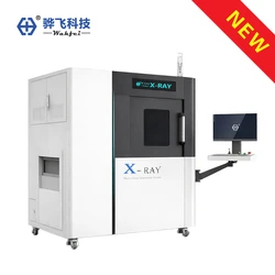
Wahfei's HF-S160 product page describes a 160 kV open-tube microfocus X-ray inspection system for SMT and semiconductor internal-defect inspection. The published information also lists up to 1000× magnification with AI super-resolution, four-axis motion, a 600 mm × 600 mm stage, a maximum payload of 20 kg, the Wahfei X-Mind system, and a dose rate below 1 μSv/h.
These published specifications describe system capability, not a universal detection limit. Whether a specific void, crack, bond-wire feature, or alignment issue can be resolved still depends on the sample, geometry, detector, recipe, and acceptance requirement. A sample trial is the correct way to verify the result.
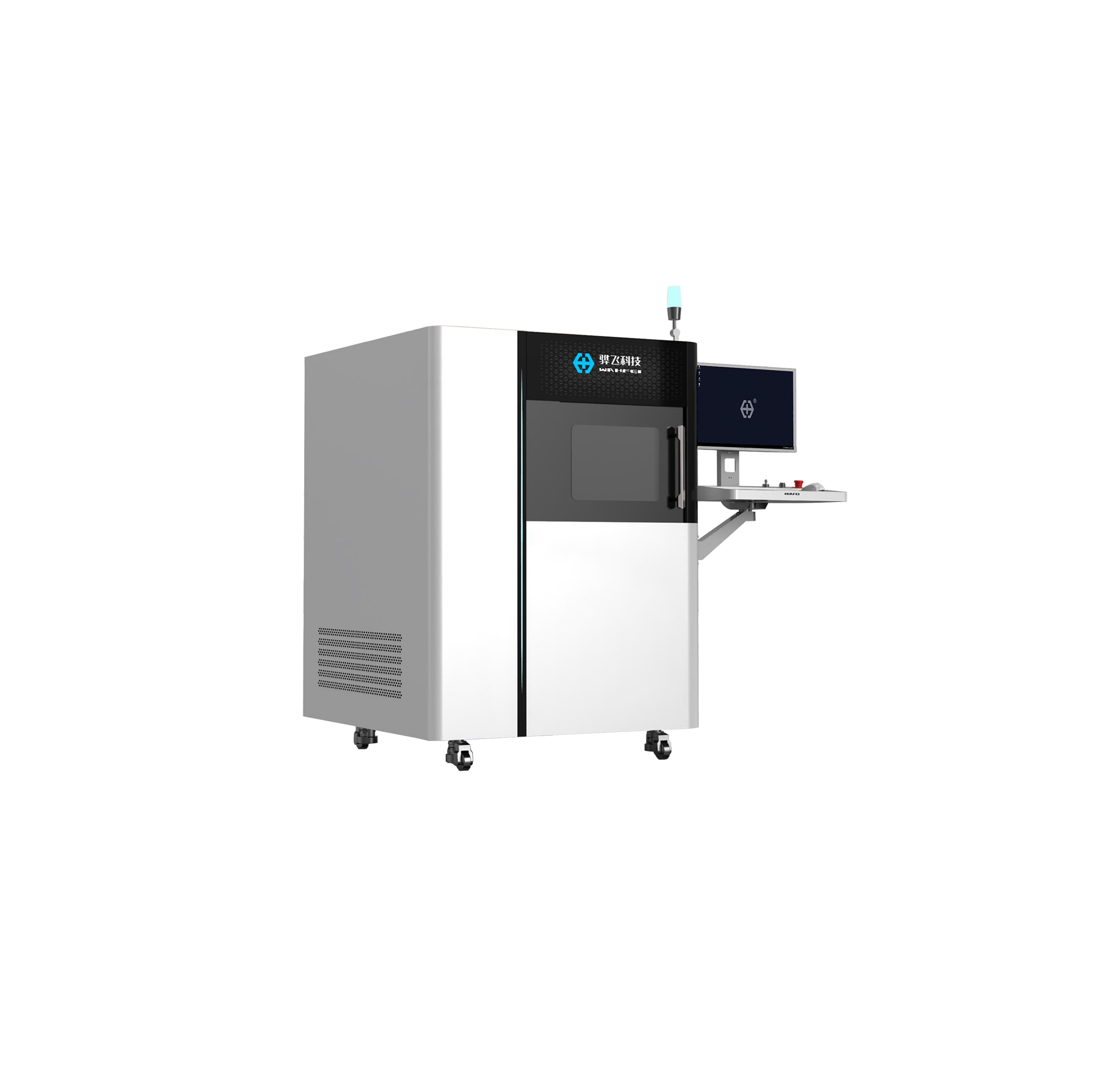
Wahfei HF-S160, an open-tube microfocus X-ray inspection system for SMT and semiconductor internal-defect inspection.
How to evaluate a system before purchase
Start with the smallest feature and the most difficult material combination that the system must inspect. Then confirm the required defect size and type; part size, thickness, and density; required image area and viewing angles; 2D, angled imaging, or 3D CT needs; expected throughput and loading method; traceability and reporting requirements; and radiation-safety documentation, training, service, and sample-testing support.
The most reliable selection process compares images from the actual product. Ask the supplier to inspect representative good samples and known defect samples, and record the conditions used for each result.
Frequently asked questions
These questions help separate a suitable system from a specification that only looks attractive on paper.
Is a microfocus X-ray system always the best choice?
No. It is a strong choice for small internal features and concealed joints, but larger or thicker parts may require more penetrating equipment. The sample and defect requirement should drive the selection.
Does higher magnification always mean higher resolution?
No. Magnification enlarges the image, but usable resolution also depends on focal spot, detector performance, geometry, motion stability, material thickness, and image processing.
Can microfocus X-ray inspection detect every defect?
No. Detection depends on defect size, orientation, material contrast, part geometry, image quality, and the inspection recipe. Sample testing is needed to establish practical capability.
Is microfocus X-ray inspection destructive?
Cabinet X-ray imaging is generally non-destructive because the product is not cut open. The product-specific process should still be reviewed if the item is sensitive to radiation or heat exposure.
Conclusion
A microfocus x-ray inspection system is valuable when a manufacturer needs to see fine internal structures without opening or damaging the product. Its small focal spot supports lower geometric blur and magnified imaging, but the final result depends on the complete system and the actual sample. The best equipment decision comes from matching source, detector, geometry, software, safety, and workflow to a defined inspection problem.
Wahfei Technology provides industrial X-ray inspection systems for electronics, semiconductor packages, batteries, connectors, and other applications. Representative sample testing can help determine whether a microfocus 2D system, an inline AXI configuration, or a 3D CT approach is appropriate for the product.