BGA ICs: Package Types, Internal Structure, and What the Term Means
BGA ICs: Package Types, Internal Structure, and What the Term Means
BGA ICs are integrated circuits supplied in a ball grid array package: conductive solder-ball terminals are arranged across the underside of the package to connect it to a printed circuit board. “BGA” describes the package interconnect format, not the chip’s function or a single internal construction. The exact package and die-connection details depend on the component design and supplier documentation.
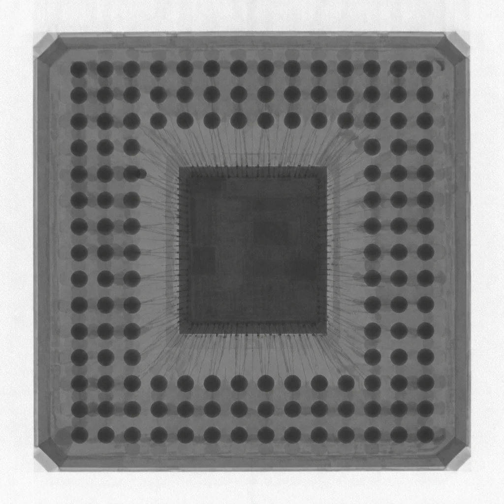
verified BGA IC package or cross-section illustration
What does BGA mean for an IC?
A BGA IC combines a semiconductor die with a package substrate and an array of external solder-ball terminals. The package routes signals and power between the die and the PCB. Because the terminals sit beneath the package body, the land pattern can support many connections within the package footprint, while the finished board-level joints are not directly visible from above.
The package code and manufacturer datasheet are the authoritative sources for a specific device’s dimensions, ball pitch, substrate, materials, and assembly limits. The term “BGA IC” alone does not identify those details.
How do BGA IC package variants differ?
BGA variants are commonly distinguished by package substrate or construction. PBGA typically refers to a plastic-substrate ball grid array; CBGA refers to a ceramic version; TBGA uses a tape-based substrate; and FCBGA denotes a flip-chip ball grid array construction. Terminology and exact definitions can vary by supplier and package family, so the device datasheet should be checked before inferring a material stack or internal interconnect.
Substrate family: affects package construction and can influence thermal-mechanical behavior.
Die-to-substrate connection: may use wire bonds or flip-chip interconnects, depending on the design.
Ball layout: pitch, count, and pattern determine the PCB land arrangement and routing constraints.
Thermal design: exposed thermal features, heat spreaders, and board-level paths vary by package.
IPC-7095E (2024) provides design and assembly process guidance for BGA technology, including component considerations and implementation issues. It is not a substitute for the package manufacturer’s device-specific data.
Why does the package format affect assembly?
BGA terminals are distributed beneath the package rather than along visible edges. Assembly therefore depends on matching the PCB land pattern and solder paste process to the exact device specification. Placement accuracy, board flatness, package warpage, moisture handling, and reflow conditions can influence joint formation.
Because the joints are covered after placement, quality teams may combine process controls, electrical testing, optical checks of accessible features, and X-ray imaging. Each method addresses different evidence: X-ray can show selected projected internal structures, while electrical testing evaluates circuit response under specified conditions.
What can X-ray show about a BGA IC?
X-ray images may help examine the BGA ball array for features such as missing positions, bridging, alignment patterns, or projected void indications. Image visibility depends on package construction, board stack-up, orientation, material thickness, detector and source geometry, and inspection settings.
A single 2D image does not reveal every internal interface or establish the IC’s functional correctness. Electrical testing is needed for electrical behavior; destructive or other analytical methods may be required for some failure investigations. No BGA package type guarantees that every defect is visible by X-ray.
How should engineers identify a BGA IC?
Start with the complete part number and the manufacturer datasheet. Confirm package designation, body dimensions, ball pitch and array, orientation mark, PCB footprint, moisture-sensitivity handling, and soldering limits. For procurement substitutions, compare the full package and assembly requirements rather than relying on a shared “BGA” label.
Understanding the package is useful because it informs board layout, assembly setup, thermal planning, and inspection choice. For a specific BGA IC, the datasheet and approved assembly documentation take precedence over generic descriptions of BGA technology.
Frequently asked questions
Is BGA an IC type? No. BGA is a package and interconnect format used by many kinds of integrated circuits.
Are all BGA ICs flip-chip devices? No. Die-to-substrate interconnection depends on the package design; the part documentation is needed to identify it.
Can X-ray identify the function of a BGA IC? No. X-ray may show selected internal structures, but it does not identify the IC’s electrical function or verify its programmed behavior.
Can one PCB footprint fit every BGA IC? No. The footprint must match the exact package dimensions, ball pitch, array, and manufacturer recommendations.
About us
Shenzhen Wahfei Technology Co.,Ltd. manufactures industrial X-ray inspection equipment. Inspection suitability for a specific BGA IC and PCB should be confirmed using representative samples.
Phone: +86 189 0297 8624 | Email: szwahfei@gmail.com | Website: https://www.szwahfei.cn/