Wire Bond Inspection in Optocouplers: What Open and Sagged Bonds Look Like on an X-ray Image
The housing is unbroken. The leads are straight. The marking is clean. None of that proves the thin wire inside — the one that joins the chip to the lead frame — is still there. A good share of optocoupler failures begin inside the package, which is exactly where the eye stops being useful.
What the Gold Wire Does Inside an Optocoupler
There is no direct electrical connection inside an optocoupler. On the input side sits a light-emitting chip; on the output side, a light-sensing chip; between them, a layer of transparent insulating material; around it all, molded plastic. A signal enters, becomes light, crosses the insulation, and turns back into current. Nothing conductive bridges input and output.
That conversion depends on the connection between the chip electrodes and the lead frame — the gold wire.
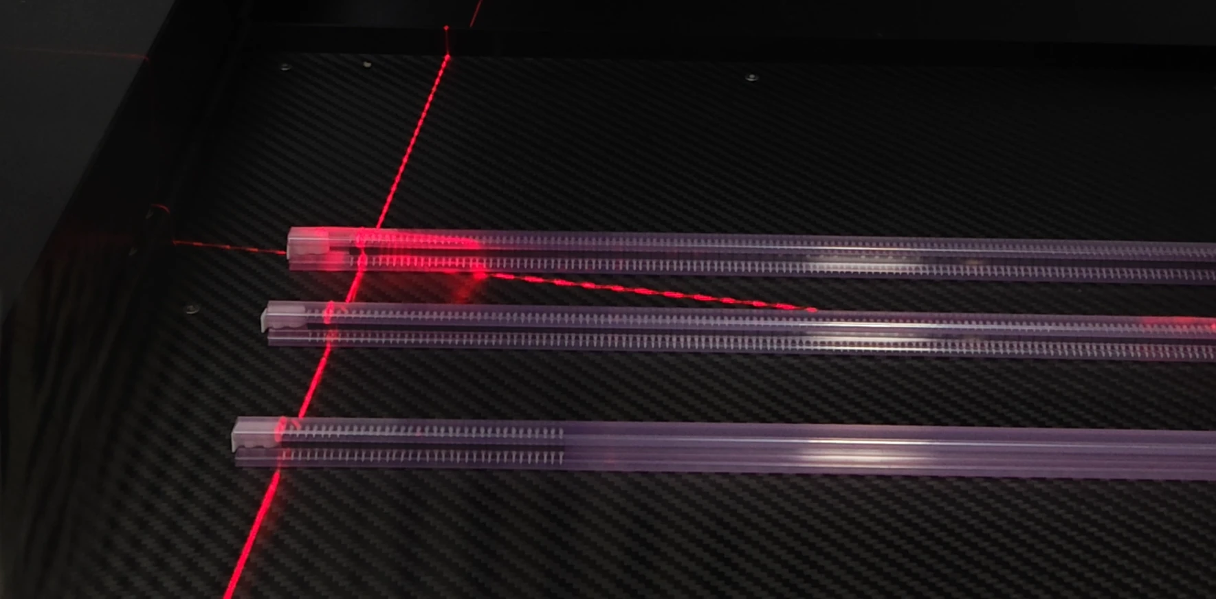
Figure 1 — Optocoupler samples, as received in a light purple tube
The wire is thin, usually somewhere between ten and a few tens of micrometers, finer than a human hair. Inside the package it hangs as an arc, welded at one end to the chip pad and at the other to a frame lead. Every step that follows can distort or break that arc: the flow of molding compound, the stress of trimming and forming, vibration during taping and shipping, the heat of insertion and soldering.
Once molding is finished, none of this is visible. No crack in the housing, no change in lead dimensions, and at room temperature the electrical readings may even look normal. With two wires, one broken one still carries the signal, and a short test may not catch it.
Two Things to Read on the Image: Is the Wire There, Is the Arc There
Plastic barely attenuates X-rays; gold, lead frame, and chip pads attenuate far more. The thick frame therefore shows up dark, the fine gold wire shows as a pale bright line, and the molding compound sits between them as light gray. Once that contrast is established, the internal structure becomes readable.
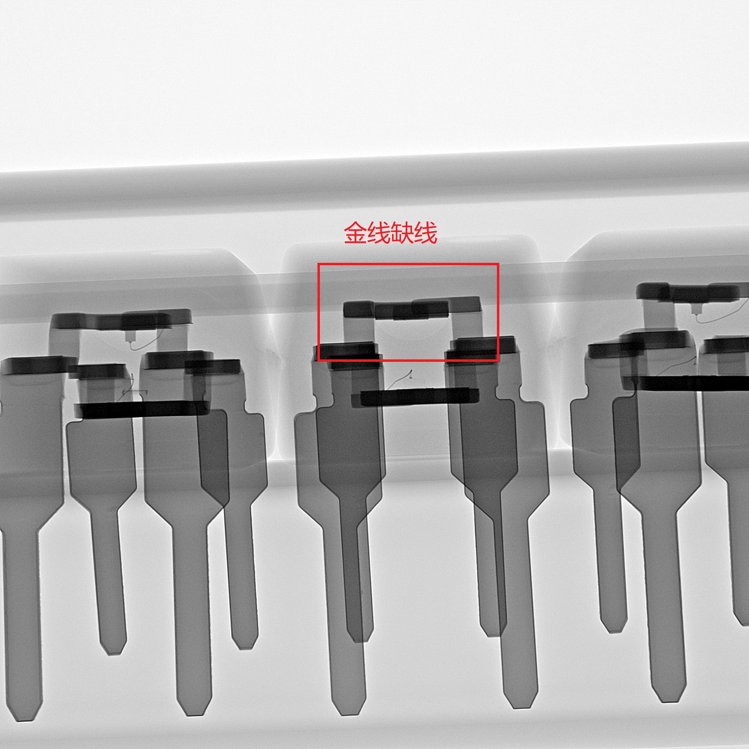
NG — Figure 2, open wire
Open wire — the arc that should run from the chip pad to the frame lead is gone along its entire length; only the two frame ends remain. The spot inside the red box is empty. Not faint — absent.
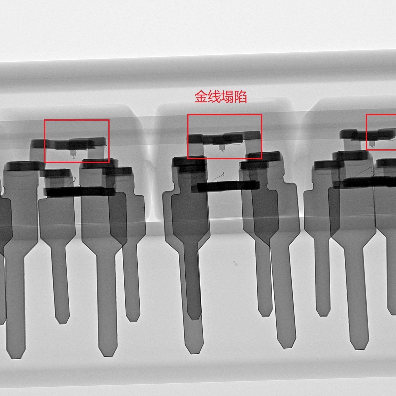
NG — Figure 3, sagging bond
Sagging — the wire is still there, but the arc has collapsed. A full curve becomes a drooping line, its height lost, a short remnant left in places. Figures 2 and 3 were taken on two different samples.
The two deserve to be read separately. An open wire is a broken connection, a functional failure. A sag is a change in geometry; the wire may not be broken at all, but it now sits closer to the structure beneath it, and part of the insulation margin has been used up. Whether that margin matters depends on the withstand-voltage design and the operating conditions of the specific part. It does not generalize.
The line between pass and fail is plain: a sound wire is complete, continuous, and holds its arc. A faulty one is either empty in the middle, or has collapsed, or is down to a remnant.
What It Replaces, and What It Cannot Replace
What it replaces is decapsulation. To see internal connections in the past, you opened the package and etched away the molding compound — and the sample was gone with it. X-ray does not damage the part: the same unit can be viewed again and again, and a whole lot can be viewed at once.
What it does not replace is electrical performance or bond strength. The image shows the shape and position of metal structures. It does not show how firmly a bond actually adhered, and it does not measure CTR, dielectric withstand, or response time. A wire that looks connected but bonded weakly will not show up as weak.
So the right place for it is not in place of final electrical test, but ahead of it: screen out the units whose structure is already clearly wrong, so that electrical test is not fighting a structural defect, and so that failure analysis starts at the moment molding ends.
As for how far off is too far — what arc height is acceptable, at what angle a deviation becomes a reject — that belongs in the quality agreement between supplier and customer. Different products, different packages, and different reliability grades take different values.
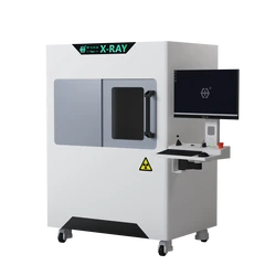
The Wahfei HF-S90 microfocus X-ray inspection system can be used for imaging internal connections in optocouplers. Specifications and functions are as published in the technical datasheet on the Wahfei website.
About Wahfei Technology — Shenzhen Wahfei Technology Co.,Ltd. designs and manufactures industrial X-ray inspection equipment, with microfocus models covering 90 kV and above. Its systems are used for non-destructive inspection in electronics manufacturing, connectors, sensors, solenoid valves and coil assemblies, semiconductor packaging, and wire and cable.
Note — The images and interpretations in this article are based on customer-supplied samples and are intended only to illustrate the inspection capability and method. Acceptance criteria are subject to the quality specification agreed between supplier and customer.