Quantifying Internal Voids in LED Lamp Beads with Micro-Focus X-Ray Inspection
Voids in the die-attach layer and the encapsulant pass every visual and electrical check — then shorten the lamp's life. Here is how they are found, and how they are measured.
The defects that pass every visual check
An LED lamp bead combines a lead frame, a die, die-attach material, bonding wires and an outer encapsulant. During die bonding and encapsulation, two void-type defects can be trapped inside the package:
• Voids in the die-attach layer shrink the effective thermal path between the die and the frame, raising the junction temperature. Over time this shows up as accelerated lumen depreciation and color shift.
• Bubbles in the encapsulant act as stress-concentration points. Under reflow soldering or thermal cycling they can trigger cracking and delamination, breaking the seal that keeps moisture out.
Both sit inside the package, and both typically pass final electrical testing. The failure appears later, in the field — which is exactly why they are expensive.
From image to number
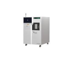
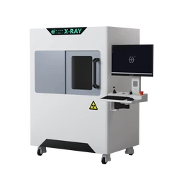
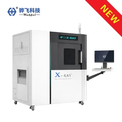
X-ray transmission imaging makes these voids visible without opening the package: denser material attenuates more radiation and appears darker, while voids attenuate less and show up as bright spots against the surrounding material. Figure 2 shows beads from the tray in Figure 1, imaged on a Wahfei HF-S81 micro-focus X-ray inspection system — lead frame, die-attach regions and voids are clearly separated. With a 5 μm focal spot, small bubbles keep sharp edges even under geometric magnification.
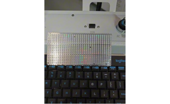
Figure 1 — Tray-loaded LED lamp beads ready for inspection
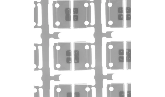
Figure 2 — X-ray image of an LED lamp bead array: lead frame, die-attach regions and voids (bright spots) are clearly separated
Seeing a void, however, is only half the job. Control requires numbers. The system's image-processing software lets the operator frame an inspection region on a bead, automatically marks the voids inside it, and reports two indicators:
• Total — the percentage of the region area occupied by all voids combined;
• Max — the percentage occupied by the single largest void, because one large void can interrupt the thermal path more severely than the same total area of dispersed small voids.
Figure 3 shows a live measurement on three regions of one bead: Region 1 reads 2.42% total / 1.92% max; Region 2 reads 0.74% / 0.74%; Region 3 reads 5.41% / 1.61% — the highest total, but dispersed rather than concentrated. Read together, the two indicators describe not only how much voiding a region contains, but how it is distributed.
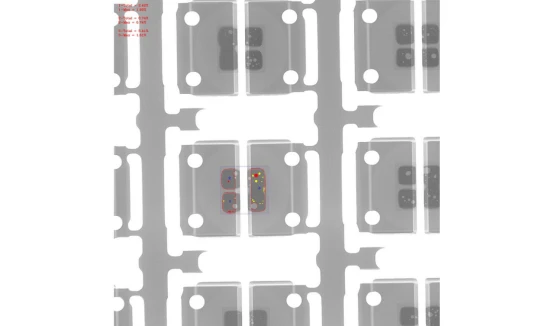
Figure 3 — Live void-rate measurement: three framed regions on one bead, with Total and Max values reported at the upper left
A note on acceptance limits: there is no industry-wide mandatory void-rate limit for LED lamp beads. Companies set Total/Max limits according to the product's application grade and customer quality agreements. What the system provides is a stable, repeatable way to measure against those limits.
Where it fits in production
• In-process sampling at packaging houses — measure void rates batch by batch and catch parameter drift in die bonding or dispensing before it spreads;
• Incoming inspection at downstream manufacturers — turn a supplier's void performance into quantified acceptance data instead of a visual impression;
• Process validation — compare die-attach materials and dispensing parameters on measured numbers;
• Failure analysis — examine returned lamps without decapsulation, keeping the evidence intact.
For tray-loaded beads, a stepping inspection program can be stored and recalled, so the same model is inspected point by point, the same way, every time.
About Wahfei Technology — Shenzhen Wahfei Technology Co.,Ltd. develops and manufactures industrial X-ray inspection systems for electronics manufacturing, semiconductor packaging and related fields. For HF-S81 specifications or a free sample evaluation, contact us at szwahfei@gmail.com or on WhatsApp at +86 189 0297 8624.
Note — The measurement data above are from a real inspection interface and are shown for illustration. Acceptance criteria for specific products are defined by the quality specifications confirmed between supplier and customer.