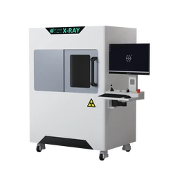
X-Ray Inspection of Sensor Internal Wiring and Solder Joints
Intermittent opens and drifting output often trace back to a wire or a solder joint hidden inside the housing. Here is how to see them before shipment.
The failure that hides inside the housing
Inside a typical sensor, the electrical path runs from the top terminal through a fine wire to a solder joint and the cable below. Damage at any point along this chain shows up as an electrical problem — but the two most vulnerable points sit inside the housing, where no visual check can reach them:
• The fine lead wire is thin and embedded in the housing or potting material. Assembly, potting, bending and vibration can stretch it thin or break it entirely, and the fracture leaves no mark on the outside.
• The solder joints at the bottom are covered by cable sleeves, heat-shrink tubing or potting compound. Insufficient solder, poor wetting and cracked joints produce no visible symptoms.
Conventional tests have clear limits here. An electrical test answers "is it conducting right now" — it cannot say whether the internal structure is already damaged, or whether it will survive the vibration and thermal cycling that come later.
What many manufacturers actually experience is this: the product ships, intermittent failures accumulate at the customer, and only the teardown of returned units reveals a broken wire or a separated joint — too late to trace the batch or the process step that caused it.
What the X-ray image shows
X-ray transmission turns the hidden structure into a grayscale image: dense materials such as metal conductors and solder absorb more radiation and appear dark, while potting compound, insulation and air appear bright. The path of the wire, the shape of the solder joints and the strands of the braided cable all become directly readable — no disassembly required.
One prerequisite matters for fine wires: image sharpness. Wahfei micro-focus systems use an X-ray source with a 5 μm focal spot, so wire edges stay sharp under geometric magnification; a larger focal spot would blur exactly the defects that need to be judged.
Figure 1 shows two customer-submitted sensor samples imaged on the same system. In one, the fine wires from the top element can be followed through their bends inside the housing, down to the braided cable at the bottom. In the other, the two wires and their solder joints appear separately, each joint a clearly defined dark blob.
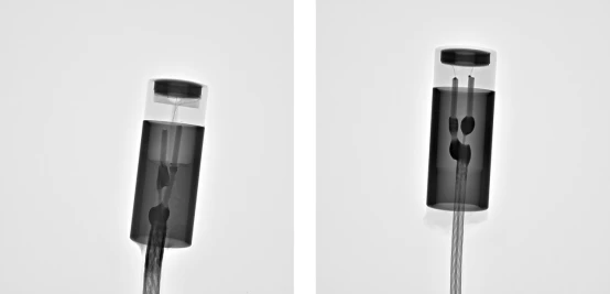
igure 1 — X-ray images of two sensor samples: internal wire paths and solder joints are directly readable
Reading the image is a matter of morphology. A sound wire is a continuous dark line of even width; a break appears as an interrupted line with mismatched edges, and necking — a wire stretched thin but not yet broken — appears as a local narrowing with lighter grayscale. Necking deserves particular attention: it can pass today's electrical test and still fail under vibration or heat.
A sound solder joint is a regular, enlarged dark region that fully covers the wire-to-cable connection; gaps, missing solder and brighter voids inside the joint all point to an unreliable connection, and joints that differ in size or shape within one unit tell the same story about process stability.
Two boundaries should be stated plainly. X-ray imaging shows the geometry of a joint, not its metallurgical wetting — a joint that looks normal in shape is not automatically a qualified joint. And because a single projection superimposes structures at different depths, a defect behind another component or close to the housing wall can be obscured; for specific samples, adding a tilted view is part of a complete inspection.
Where it fits in production
• Sampling without destruction — inspected units continue through the normal flow and can be re-checked or archived for comparison;
• Interception before shipment — catch structural damage before it becomes intermittent field failures, returns and repairs;
• Process correlation — if necked wires cluster around one bending station or undersized joints around one soldering machine, the images point directly at the process step;
• A complement to electrical testing — the electrical test confirms continuity today; the image confirms structural integrity. Reliability judgments need both.
The same "fine wire plus solder joint" inspection need exists in connectors and terminal blocks, wire harnesses, relays and switches, and potted electronic modules of all kinds — anywhere the connection point is the functional heart of the product, hidden behind a housing.
About Wahfei Technology — Shenzhen Wahfei Technology Co.,Ltd. develops and manufactures industrial X-ray inspection systems, including micro-focus models widely used in electronics manufacturing, sensors, connectors and cable assemblies. Sample evaluation is welcome — real images help you judge capability and select the right model. Contact us at szwahfei@gmail.com or on WhatsApp at +86 189 0297 8624.
Note — The images are from customer-submitted samples, anonymized, and are shown to illustrate the inspection method. Acceptance criteria for specific products are defined by the quality specifications confirmed between supplier and customer.