PCB X-ray inspection for blind and buried via defects
Blind and buried vias help printed circuit boards route signals through dense layer stacks without using every layer. Their position inside the board, however, makes inspection different from checking a visible surface feature. X-ray images can reveal useful evidence, but an image should be interpreted in the context of the via design and the inspection question.
What makes a via blind or buried?
A blind via connects an outer layer to one or more inner layers, ending within the board rather than passing through its full thickness. A buried via connects internal layers and is enclosed by the board’s outer layers. Both structures may be formed, filled, or capped in different ways depending on the stack-up and fabrication process. Design data and fabrication records help establish where the feature should be and what its intended geometry is.
What a 2D X-ray projection can show
A 2D X-ray projection may show the via’s apparent location and continuity, relative density, and conspicuous changes such as a void-like region, an interruption, or an irregular outline. It can also help compare repeated features across a board. These are image-based indications, not automatic proof of a defect or a complete description of the via’s internal shape.
Projection images collapse depth into a single view. Vias, copper features, planes, and other structures along the beam path can overlap. A feature may be hidden, appear wider or denser than it is, or be difficult to assign to a particular layer. A single view therefore cannot reliably resolve every suspected condition, especially in a dense stack-up.
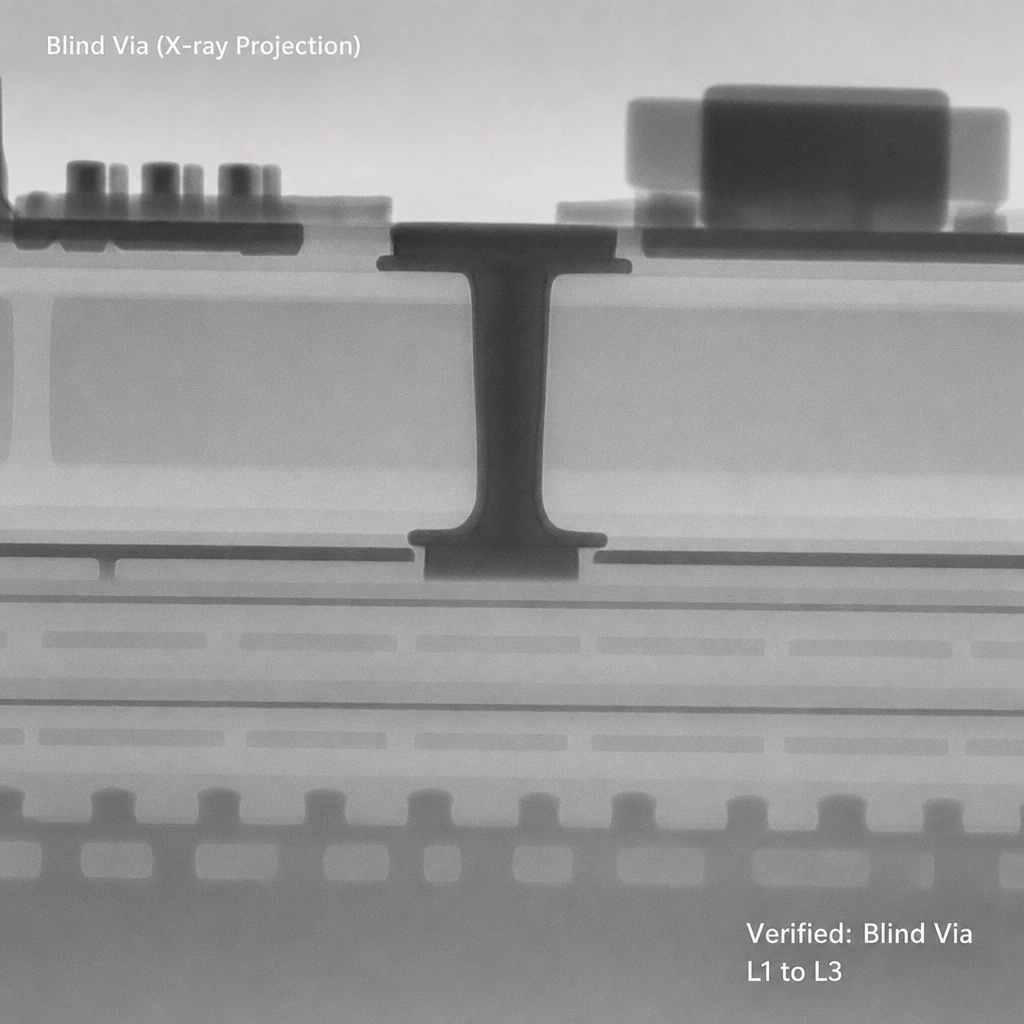
a verified X-ray image of a blind via with confirmed context
When to use another method
Consider CT when depth separation or a three-dimensional view is needed to investigate overlapping structures. CT can add spatial context, but interpretation still depends on image quality, material geometry, and the inspection objective. For direct examination of internal construction or a suspected local material condition, a microsection can expose the relevant cross-section; it is destructive and samples a limited location.
Electrical testing can help determine whether a connection behaves as intended, but it does not by itself identify the physical cause or exact location of an anomaly. When a finding matters to a release or root-cause decision, combine appropriate methods: use X-ray to locate and screen, then select CT, microsection, electrical testing, or a combination according to the unresolved question. Correlate results with the stack-up, design files, and manufacturing history, and state clearly what the evidence does and does not establish.