



Industrial X-Ray Inspection of Wafers: Precision and Non-Destructive Testing Safeguarding Core Semiconductor Quality
In the semiconductor manufacturing sector, wafers serve as the cornerstone of chip production. Their microscopic defects—such as scratches, cracks, or internal voids—often lie hidden beneath the surface, where even minor oversights can render an entire batch of products unusable. Industrial X-ray wafer inspection technology, with its non-contact, non-destructive, and high-resolution capabilities, emerges as the solution.
View More
2025-12-15
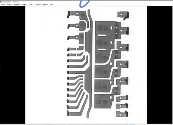
X-Ray Inspection Equipment Empowers IC Packaging Quality Control
The internal structure of chips is highly intricate, with diverse packaging forms and complex manufacturing processes. For IDMs, packaging and testing facilities, solution designers, and end-brand manufacturers alike, the core requirement in quality management and reliability verification has become the rapid and accurate detection of packaging defects and process risks without damaging the devices. Against this backdrop, X-Ray non-destructive testing equipment has emerged as a vital tool for packaging quality control and failure analysis (FA).
View More
2025-12-09
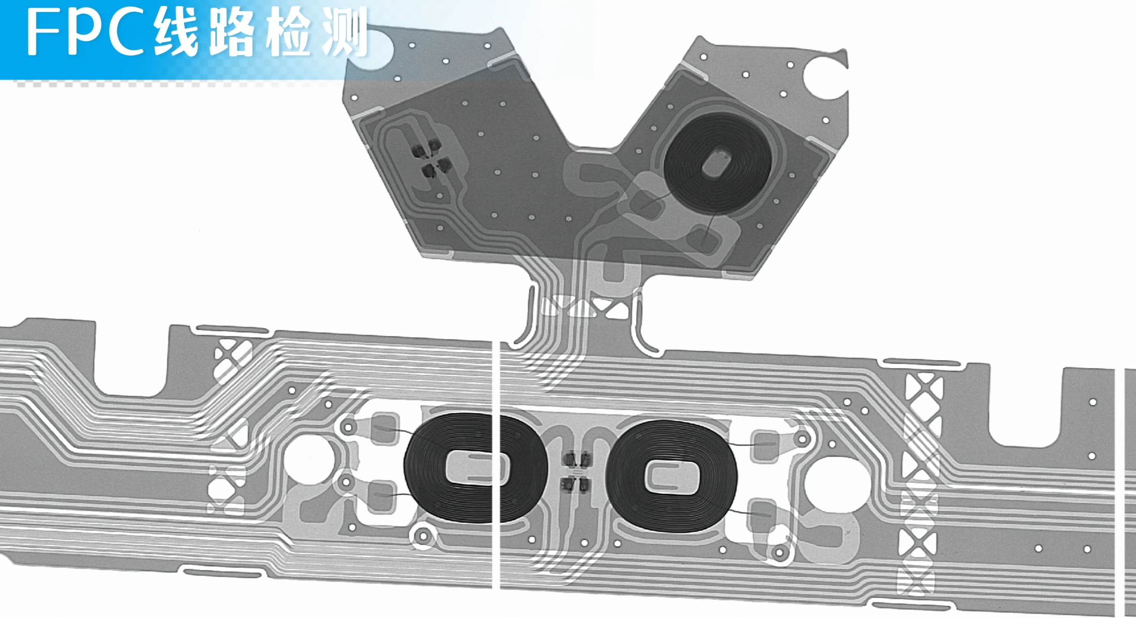
X-Ray Non-Destructive Testing for FPC Circuits
X-Ray Testing System Real-Time Imaging Interface / High-Resolution X-Ray Imaging Clearly Reveals FPC Internal Structure
View More
2025-12-02
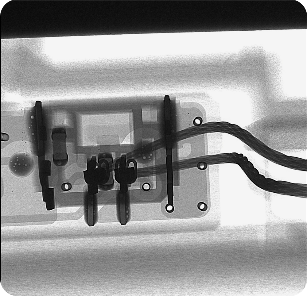
X-Ray Inspection of Injection-Molded Parts · Live Demonstration of Foreign Object Detection in Metal Power Enclosures
During the production of injection‑molded parts and metal power enclosures, foreign object contamination is often hidden and unpredictable, impacting both yield and safety. With high‑resolution imaging technology, metallic debris, plastic residue, assembly omissions, and other internal defects can be precisely located without cracking or damaging the sample structure, helping manufacturers identify risks in time and maintain stable production quality.
View More
2025-11-29

Core Considerations for Procuring X-Ray Inspection Equipment
In the fields of electronics manufacturing, integrated circuit packaging, automotive parts, and precision casting inspection, X-Ray equipment has become a critical tool for quality control. However, many companies focus excessively on hardware parameters when purchasing equipment, while overlooking a core fact: under the same shooting conditions, image processing technology is the key factor that determines inspection results.
View More
2025-11-17
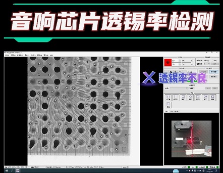
X-ray Inspection Audio Chip Solder Penetration Rate Video Demonstration
X-ray Determination of Common Defects and Countermeasures: Insufficient Solder Penetration (Shallow Fill): Increase preheat, adjust wave contact angle and time, optimize hole wall cleanliness. Internal Voids/Gas Entrapment: Reduce solder gas content, optimize flux volatilization path and nitrogen protection. Eccentric Wetting: Check pin centering and fixture positioning, perform hole chamfering/expand ring width if necessary.
View More
2025-10-25
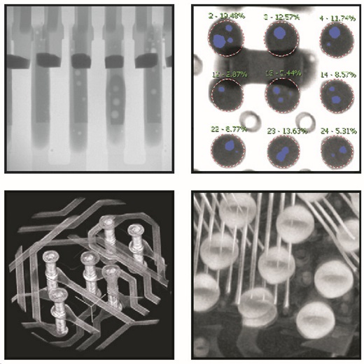
PCBA X-Ray Inspection Technology and Solder Defect Analysis
X-rays possess extremely strong penetrating power. Different material densities and thicknesses absorb X-rays to varying degrees. By analyzing the intensity changes of X-rays after passing through a sample, grayscale contrast images are formed to identify internal structures. Based on material density characteristics, PCBA components can be divided into four categories: tin-lead alloy solder joints (high density, appear dark in images); metal packaging shells, ceramic packaging, chips (medium density); plastic packaging materials, silicon materials (low density, appear light in images); void, crack defects and PCB vias (X-rays pass through completely, appear brightest).
View More
2025-10-10