


The Mandatory Final Check: X-Ray for Zero-Defect PCBA Manufacturing
Can't inspect hidden solder joints? X-Ray inspection is your final quality gate. Learn how it visualizes BGA balls, measures voiding, and prevents costly escapes in network, security, and industrial control hardware before shipment.
View More
2026-01-16
X-Ray Automated Inspection for Internal Product Defects - Solving Inspection Challenges for BGAs, IGBTs
Simple operation allows even non-technical users to get started quickly. One-click detection identifies internal defects such as BGA solder joint failures, IGBT bubbles, and PCB solder bridges. Boost inspection efficiency with MES system integration to reduce scrap rates and labor costs.
View More
2026-01-15
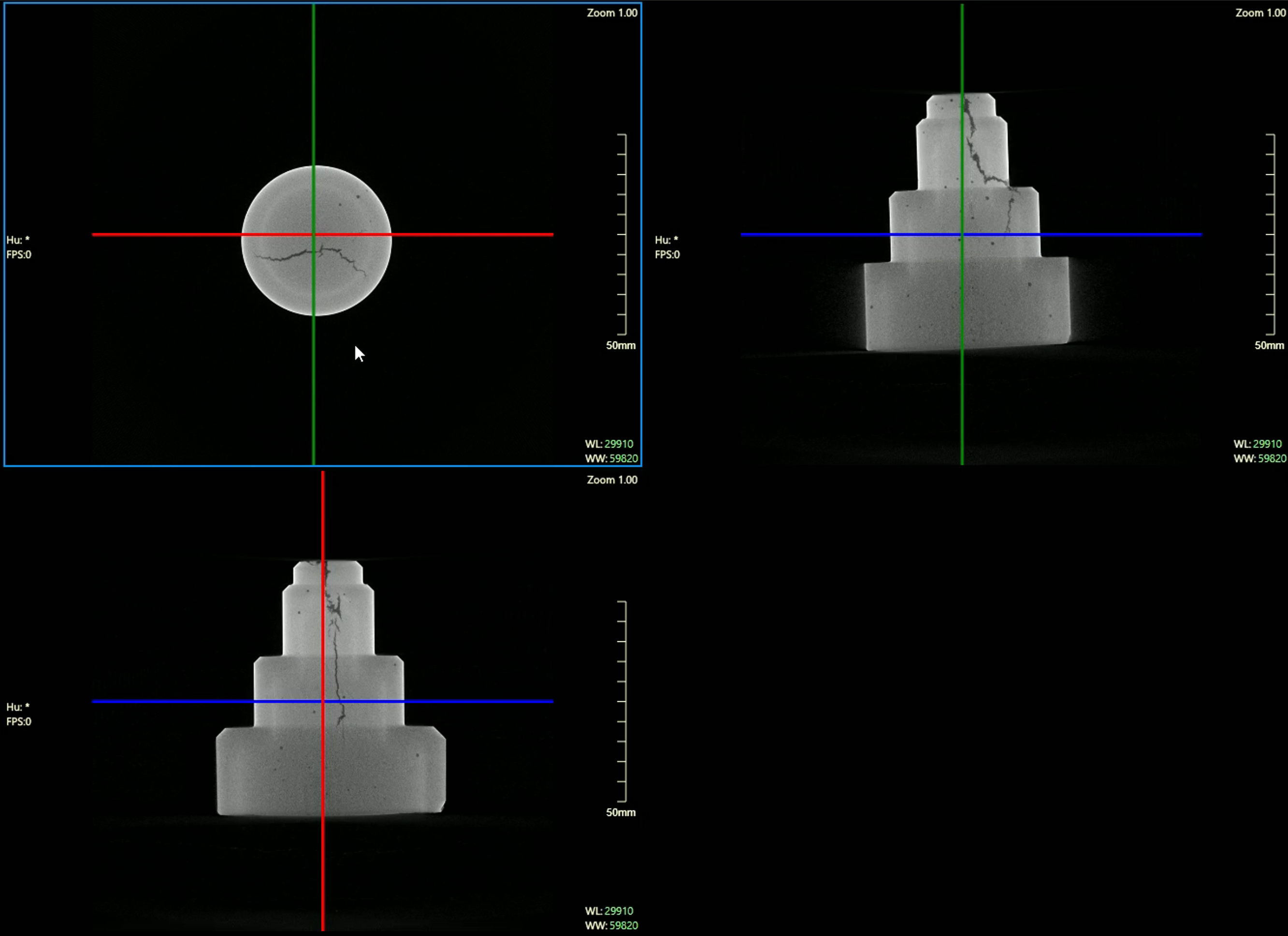
X-Ray CT Inspection of Silicon Carbide Cracks and Inclusions
Unlike the stacking effect of conventional radiographic images, 3D CT (Computed Tomography) technology uses 360-degree rotational imaging combined with algorithmic reconstruction to perform “layer-by-layer slicing” analysis of SiC wafers and power devices with micron-level precision.
View More
2026-01-06
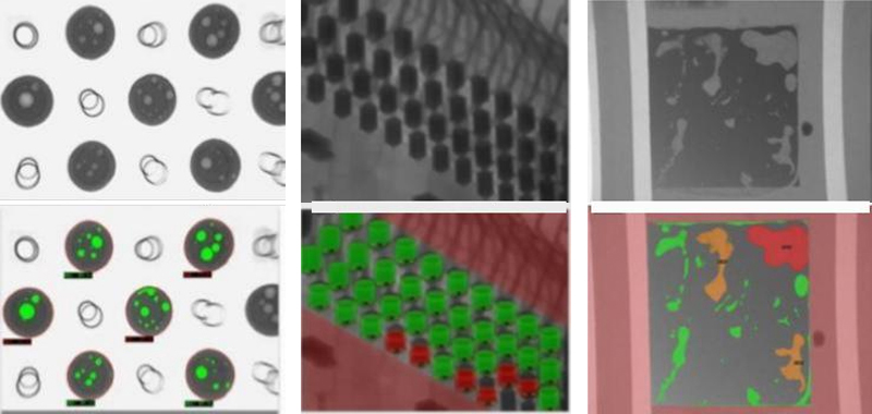
Industrial X-Ray Inspection for LED Eutectic Solder Bridging
In high-end LED packaging processes, eutectic bonding is widely adopted for its excellent thermal conductivity and long-term reliability. However, as chip dimensions continue to shrink, process control becomes exponentially more challenging. Solder bridging can cause electrical short circuits, while voiding leads to thermal dissipation failure. These defects, hidden beneath the chip interface, are among the primary causes of latent product failure. When dealing with micron-level internal defects, high-penetration, high-resolution X-Ray inspection technology becomes the critical safeguard for outgoing product quality.
View More
2025-12-29
X-Ray Inspection of BGA Defects | Video Demonstration
Wahfei's X-Ray inspection system is specifically designed for this purpose. The system offers real-time, off-axis X-Ray imaging, specially tailored for the inspection of PCBA (Printed Circuit Board Assembly) and array-type devices. It is suitable for use both in production lines and in failure analysis laboratories. The sample can be rotated 360° and supports large tilt viewing angles; combined with an intuitive software interface, it enables operators to clearly observe and identify even the most challenging defect types.
View More
2025-12-27
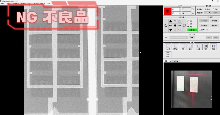
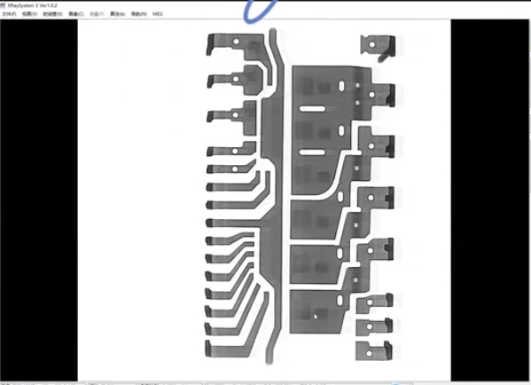
Industrial X-Ray Inspection for SMD and FPC Assemblies with Hidden Solder Joints
For products such as SMD and FPC assemblies with complex structures and hidden solder joints,industrial X-ray inspection is no longer just a supplementary quality control method.It can be integrated as a core inspection process, enabling manufacturers to identify internal soldering defects before shipment and effectively reduce hidden quality risks.
View More
2025-12-24
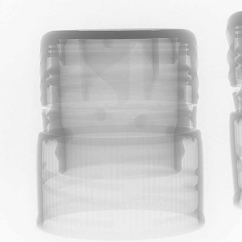
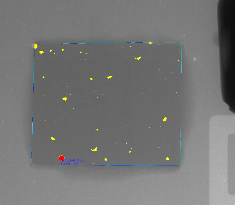
X-Ray Inspection for High-End Cosmetics like Lipsticks and Liquid Lip Tints & Plastic Packaging
Traditional inspection methods often rely on manual sampling or destructive unpacking. This is not only inefficient but also fails to cover every product leaving the factory. Especially for items with composite plastic and metal packaging, such as lipsticks and liquid lip tints, how to inspect the internal condition without opening, touching, or damaging the exterior has become an industry pain point. This is exactly where modern industrial X-ray inspection equipment comes into play. Leveraging the strong penetrative power and density resolution of X-rays, we can conduct a thorough “CT scan” of each product, examining it from the inside out.
View More
2025-12-19
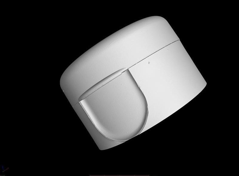
Why is industrial X-Ray computed tomography (CT) particularly well-suited for inspecting injection-molded parts?
Random sampling, prototyping, first article inspection (FAI), and mold geometry optimization each have distinct inspection objectives requiring different types of analysis. X-ray CT systems and high-quality standard X-ray solutions deliver a wide range of results.
View More
2025-12-17
Industrial X-Ray Inspection of Wafers: Precision and Non-Destructive Testing Safeguarding Core Semiconductor Quality
In the semiconductor manufacturing sector, wafers serve as the cornerstone of chip production. Their microscopic defects—such as scratches, cracks, or internal voids—often lie hidden beneath the surface, where even minor oversights can render an entire batch of products unusable. Industrial X-ray wafer inspection technology, with its non-contact, non-destructive, and high-resolution capabilities, emerges as the solution.
View More
2025-12-15
X-Ray Inspection Equipment Empowers IC Packaging Quality Control
The internal structure of chips is highly intricate, with diverse packaging forms and complex manufacturing processes. For IDMs, packaging and testing facilities, solution designers, and end-brand manufacturers alike, the core requirement in quality management and reliability verification has become the rapid and accurate detection of packaging defects and process risks without damaging the devices. Against this backdrop, X-Ray non-destructive testing equipment has emerged as a vital tool for packaging quality control and failure analysis (FA).
View More
2025-12-09
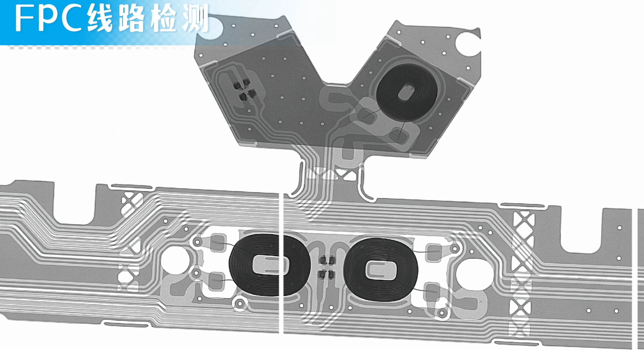
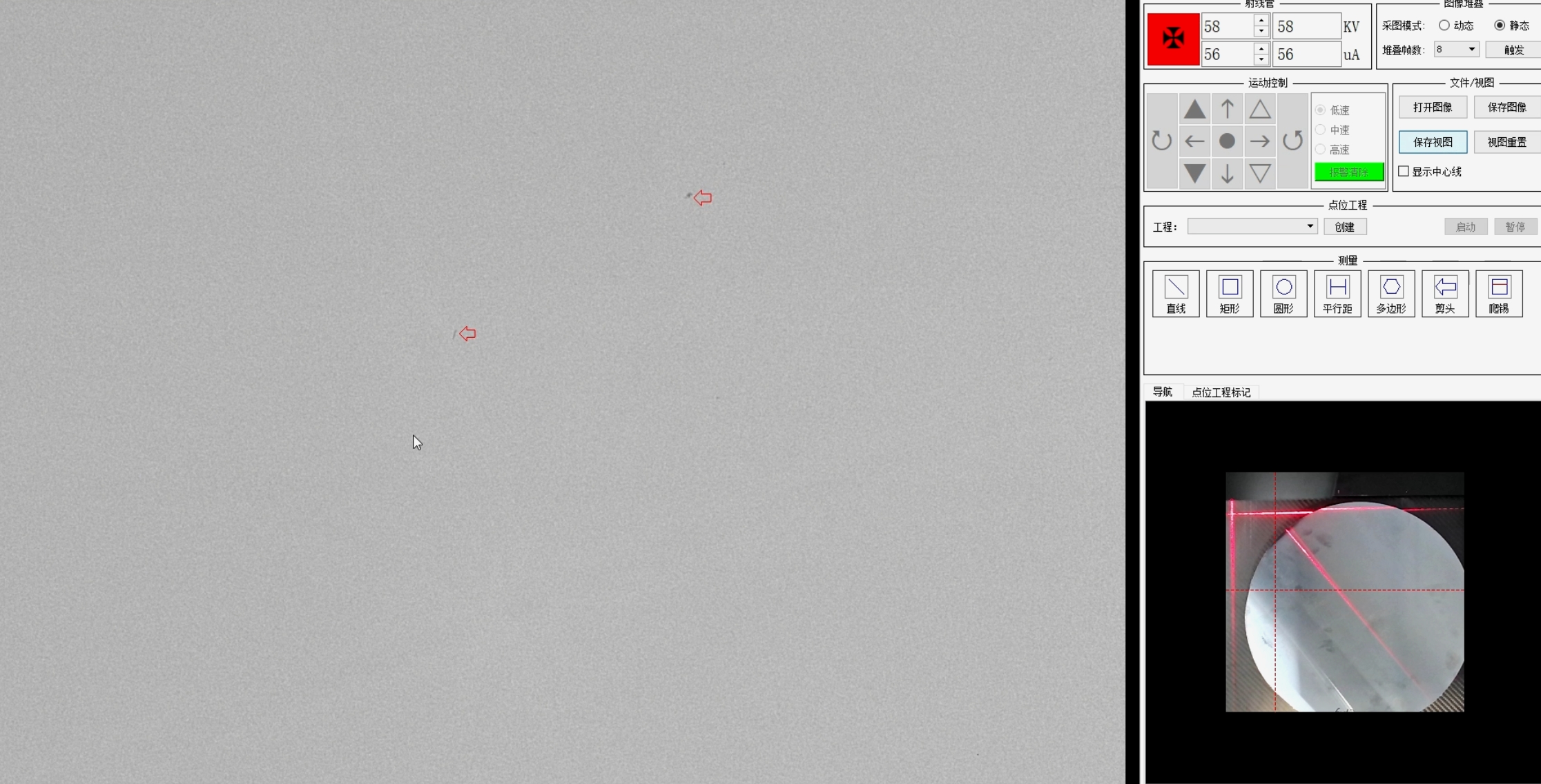
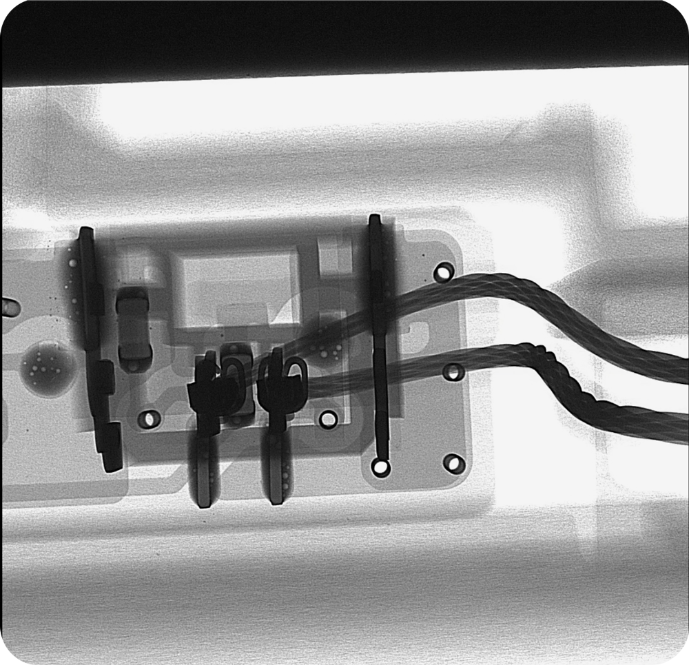
X-Ray Non-Destructive Testing for FPC Circuits
X-Ray Testing System Real-Time Imaging Interface / High-Resolution X-Ray Imaging Clearly Reveals FPC Internal Structure
View More
2025-12-02
X-Ray Inspection of Injection-Molded Parts · Live Demonstration of Foreign Object Detection in Metal Power Enclosures
During the production of injection‑molded parts and metal power enclosures, foreign object contamination is often hidden and unpredictable, impacting both yield and safety. With high‑resolution imaging technology, metallic debris, plastic residue, assembly omissions, and other internal defects can be precisely located without cracking or damaging the sample structure, helping manufacturers identify risks in time and maintain stable production quality.
View More
2025-11-29